JAJSIW7A April 2020 – January 2021 LM5181
PRODUCTION DATA
- 1 特長
- 2 アプリケーション
- 3 概要
- 4 Revision History
- 5 概要 (続き)
- 6 Pin Configuration and Functions
- 7 Specifications
-
8 Detailed Description
- 8.1 Overview
- 8.2 Functional Block Diagram
- 8.3
Feature Description
- 8.3.1 Integrated Power MOSFET
- 8.3.2 PSR Flyback Modes of Operation
- 8.3.3 Setting the Output Voltage
- 8.3.4 Control Loop Error Amplifier
- 8.3.5 Precision Enable
- 8.3.6 Configurable Soft Start
- 8.3.7 External Bias Supply
- 8.3.8 Minimum On-Time and Off-Time
- 8.3.9 Overcurrent Protection
- 8.3.10 Thermal Shutdown
- 8.4 Device Functional Modes
-
9 Application and Implementation
- 9.1 Application Information
- 9.2
Typical Applications
- 9.2.1
Design 1: Wide VIN, Low IQ PSR Flyback Converter Rated at 5 V, 0.5 A
- 9.2.1.1 Design Requirements
- 9.2.1.2
Detailed Design Procedure
- 9.2.1.2.1 Custom Design With WEBENCH® Tools
- 9.2.1.2.2 Custom Design With Excel Quickstart Tool
- 9.2.1.2.3 Flyback Transformer – T1
- 9.2.1.2.4 Flyback Diode – DFLY
- 9.2.1.2.5 Zener Clamp Circuit – DF, DCLAMP
- 9.2.1.2.6 Output Capacitor – COUT
- 9.2.1.2.7 Input Capacitor – CIN
- 9.2.1.2.8 Feedback Resistor – RFB
- 9.2.1.2.9 Thermal Compensation Resistor – RTC
- 9.2.1.2.10 UVLO Resistors – RUV1, RUV2
- 9.2.1.2.11 Soft-Start Capacitor – CSS
- 9.2.2 Application Curves
- 9.2.1
Design 1: Wide VIN, Low IQ PSR Flyback Converter Rated at 5 V, 0.5 A
- 10Power Supply Recommendations
- 11Layout
- 12Device and Documentation Support
- 13Mechanical, Packaging, and Orderable Information
9.2.1.2.4 Flyback Diode – DFLY
The flyback diode reverse voltage is given by Equation 19.
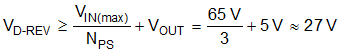
Select a 40-V, 3-A Schottky diode for this application to account for inevitable diode voltage overshoot and ringing related to the resonance of transformer leakage inductance and diode parasitic capacitance. Connect an appropriate RC snubber circuit (for example, 100 Ω and 22 pF) across the flyback diode if needed.
In general, choose a flyback diode with current rating greater than the maximum peak secondary winding current of NPS × ISW-PEAK. As mentioned in Section 11, place adequate copper at the cathode of the diode to improve its thermal performance and prevent overheating during high ambient temperature or overload conditions. Beware of the high leakage current typical of a Schottky diode at elevated operating temperatures.