JAJSLO9D June 2015 – May 2021 LM53600-Q1 , LM53601-Q1
PRODUCTION DATA
- 1 特長
- 2 アプリケーション
- 3 概要
- 4 Revision History
- 5 Device Comparison
- 6 Pin Configuration and Functions
- 7 Specifications
- 8 Detailed Description
- 9 Applications and Implementation
- 10Power Supply Recommendations
- 11Layout
- 12Device and Documentation Support
- 13Mechanical, Packaging, and Orderable Information
パッケージ・オプション
メカニカル・データ(パッケージ|ピン)
- DSX|10
サーマルパッド・メカニカル・データ
- DSX|10
発注情報
8.3.5 RESET Function
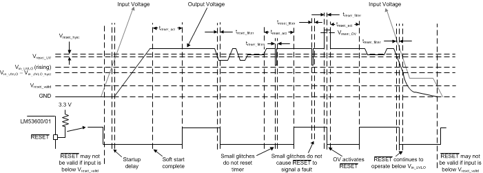
While the reset function of the LM53600-Q1 and LM53601-Q1 devices resembles a standard power good function, its functionality is designed to replace a discrete reset IC, reducing BOM cost. There are three major differences between the reset function and the normal power good function seen in most regulators:
- A delay has been added for release of reset. See waveforms below.
- RESET output signals a fault (pulls its output to ground) while the part is disabled.
- RESET continues to operate with input voltage as low as 1.5 V. Below this input voltage, RESET output may be high impedance.
 Figure 8-5 Reset Output Function Operation
The following table summarizes conditions that cause a fault to be flagged by RESET . Once a fault is flagged, RESET will not be released (become high impedance) until either there is no fault for treset_act or VIN drops below Vreset_valid.
Table showing conditions that cause RESET to signal a fault (pull low).
| FAULT CONDITION INITIATED | FAULT CONDITION ENDS (AFTER WHICH Treset_act MUST PASS BEFORE RESET OUTPUT IS RELEASED) |
|---|---|
| FB below Vreset_UV for longer than treset_filt | FB above Vreset_UV + Vreset_hyst for longer than treset_filt |
| FB above Vreset_OV for longer than treset_filt | FB below Vreset_OV - Vreset_hyst for longer than treset_filt |
| Junction temperature exceeds TSD | Junction temperature falls below TSD – TSD_hyst |
| EN low | tEN passes after EN becomes high(1) |
| VIN falls below Vin_UVLO - Vin_UVLO _hyst or VCC pin falls below Vcc_UVLO - Vcc_UVLO_hyst | Voltage on VIN exceeds Vin_UVLO and VCC exceed Vcc_UVLO |
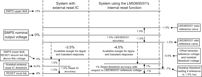
The threshold voltage for the RESET function is specified taking advantage of the availability of the LM53600-Q1 internal feedback threshold to the RESET circuit. This allows a maximum threshold of 97% of selected output voltage to be specified at the same time as 95.7% of actual operating point. The net result is a more accurate reset function while expanding the system allowance for transient response without the need for extremely accurate internal circuitry. See output voltage error stack up comparison, below.
 Figure 8-6 Reset Threshold Voltage Stack Up