JAJSCV5 November 2016 LM53602 , LM53603
PRODUCTION DATA.
- 1 特長
- 2 アプリケーション
- 3 概要
- 4 改訂履歴
- 5 Device Comparison Table
- 6 Pin Configuration and Functions
- 7 Specifications
- 8 Detailed Description
- 9 Application and Implementation
- 10Power Supply Recommendations
- 11Layout
- 12デバイスおよびドキュメントのサポート
- 13メカニカル、パッケージ、および注文情報
7 Specifications
7.1 Absolute Maximum Ratings
over the recommended operating junction temperature range of –40°C to 150°C (unless otherwise noted)(1)| PARAMETER | MIN | MAX | UNIT |
|---|---|---|---|
| VIN to AGND, PGND(2) | –0.3 | 40 | V |
| SW to AGND, PGND(3) | –0.3 | VIN + 0.3 | V |
| CBOOT to SW | –0.3 | 3.6 | V |
| EN to AGND, PGND(2) | –0.3 | 40 | V |
| BIAS to AGND, PGND | –0.3 | 16 | V |
| FB to AGND, PGND : fixed 5 V and 3.3 V | –0.3 | 16 | V |
| FB to AGND, PGND : ADJ | –0.3 | 5.5 | V |
| RESET to AGND, PGND | –0.3 | 8 | V |
| SYNC, FPWM, to AGND, PGND | –0.3 | 5.5 | V |
| VCC to AGND, PGND | –0.3 | 4.2 | V |
| RESET pin current(4) | –0.1 | 1.2 | mA |
| AGND to PGND(5) | –0.3 | 0.3 | V |
| Storage temperature, Tstg | –40 | 150 | °C |
(1) Stresses beyond those listed under Absolute Maximum Ratings may cause permanent damage to the device. These are stress ratings only, which do not imply functional operation of the device at these or any other conditions beyond those indicated under Recommended Operating Conditions. Exposure to absolute-maximum-rated conditions for extended periods may affect device reliability. Values given are D.C.
(2) A maximum of 42 V can be sustained at this pin for a duration of ≤ 500 ms at a duty cycle of ≤ 0.01%.
(3) Transients on this pin, not exceeding –3 V or +40 V, can be tolerated for a duration of ≤ 100 ns. For transients between 40 V and 42 V, see note (2).
(4) Positive current flows into this pin.
(5) A transient voltage of ±2 V can be sustained for ≤1 µs.
7.2 ESD Ratings
| VALUE | UNIT | ||||
|---|---|---|---|---|---|
| V(ESD) | Electrostatic discharge | Human-body model (HBM), per ANSI/ESDA/JEDEC JS-001(1) | Pins 1, 2, 3, 12, 13, | ±1500 | V |
| Pins 11, 5, 8, 9, 6, 7, 4 | ±2500 | ||||
| Charged-device model (CDM), per JEDEC specification JESD22-C101(2) | Pins 3, 4, 5, 6, 7, 11, 12 and 13 | ±750 | |||
| Pins 1, 2, 8, 9, 15 and 16 | ±500 | ||||
(1) JEDEC document JEP155 states that 500-V HBM allows safe manufacturing with a standard ESD control process.
(2) JEDEC document JEP157 states that 250-V CDM allows safe manufacturing with a standard ESD control process.
7.3 Recommended Operating Conditions
over the recommended operating junction temperature range of –40°C to 150°C (unless otherwise noted)| MIN | NOM | MAX | UNIT | ||
|---|---|---|---|---|---|
| Input voltage(3) | 3.9 | 36 | V | ||
| Output voltage : fixed 5 V(1) | 0 | 5 | V | ||
| Output voltage : fixed 3.3 V(1) | 0 | 3.3 | V | ||
| Output voltage adjustment range: ADJ(1)(2) | 3.3 | 10 | V | ||
| Output current for LM53603 | 0 | 3 | A | ||
| Output current for LM53602 | 0 | 2 | A | ||
| RESET pin current | 0 | 1 | mA | ||
| Operating junction temperature(4) | –40 | 150 | °C | ||
(1) Under no conditions should the output voltage be allowed to fall below zero volts.
(2) An extended output voltage range to 10 V is possible with changes to the typical application schematic. Also, some system specifications are not achieved for output voltages greater than 6 V. Consult the factory for further information.
(3) See System Characteristics for details of input voltage range.
(4) High junction temperatures degrade operating lifetimes. Operating lifetime is de-rated for junction temperatures greater than 125°C.
7.4 Thermal Information
| THERMAL METRIC(1) | LM53603, LM53602 | UNIT | |
|---|---|---|---|
| PWP (HTSSOP) | |||
| 16 PINS | |||
| RθJA | Junction-to-ambient thermal resistance | 42.5 | °C/W |
| RθJC(top) | Junction-to-case (top) thermal resistance | 22.6 | °C/W |
| RθJB | Junction-to-board thermal resistance | 16.2 | °C/W |
| ψJT | Junction-to-top characterization parameter | 0.6 | °C/W |
| ψJB | Junction-to-board characterization parameter | 16.0 | °C/W |
| RθJC(bot) | Junction-to-case (bottom) thermal resistance | 1.1 | °C/W |
(1) The values given in this table are only valid for comparison with other packages and cannot be used for design purposes. These values were calculated in accordance with JESD 51-7, and simulated on a 4-layer JEDEC board. They do not represent the performance obtained in an actual application. For design information please see the Maximum Ambient Temperature section. For more information about traditional and new thermal metrics, see the Semiconductor and IC Package Thermal Metrics application report and the Using New Thermal Metrics (SBVA025) application report.
7.5 Electrical Characteristics
Limits apply to the recommended operating junction temperature range of –40°C to 150°C, unless otherwise noted. Minimum and maximum limits are verified through test, design, or statistical correlation. Typical values represent the most likely parametric norm at TJ = 25°C, and are provided for reference purposes only. Unless otherwise stated the following conditions apply: VIN = 13.5 V.| PARAMETER | TEST CONDITIONS | MIN(1) | TYP | MAX(1) | UNIT | |
|---|---|---|---|---|---|---|
| VFB | Initial reference voltage accuracy for 5-V and 3.3-V options | VIN = 3.8 V to 36 V, FPWM, TJ = 25°C |
–1% | 1% | ||
| VIN = 3.8 V to 36 V, FPWM | –1.25% | 1.25% | ||||
| VREF | Reference voltage for ADJ option | VIN = 3.8 V to 36 V, FPWM, TJ = 25°C |
0.993 | 1 | 1.007 | V |
| VIN = 3.8 V to 36 V, FPWM, TJ = –40°C to 125°C |
0.99 | 1 | 1.01 | |||
| VIN-operate | Minimum input voltage to operate(2) | Rising | 3.2 | 3.95 | V | |
| Falling | 2.9 | 3.55 | ||||
| Hysteresis, below | 0.34 | |||||
| IQ | Operating quiescent current; measured at VIN pin(3)(4) | VBIAS = 5 V, TJ = –40°C to 125°C |
8 | 13 | µA | |
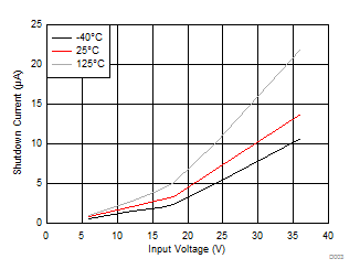
| ISD | Shutdown quiescent current; measured at VIN pin | EN ≤ 0.4 V, TJ = 25°C | 1.7 | µA | ||
| EN ≤ 0.4 V, TJ = 125°C | 3.5 | |||||
| IB | Current into the BIAS pin(4) | VBIAS = 5 V, FPWM = 3.3 V | 47 | 78 | µA | |
| IEN | Current into EN pin | VIN = VEN = 13.5 V | 2.3 | µA | ||
| IFB | Bias current into FB pin | ADJ option | 10 | nA | ||
| VRESET | RESET upper threshold voltage | Rising, % of nominal Vout | 105% | 107% | 110% | |
| RESET lower threshold voltage | Falling, % of nominal Vout | 92% | 94% | 96.5% | ||
| RESET lower threshold voltage with respect to output voltage | Falling, % actual Vout | 94.5% | 95.7% | |||
| VRESET-Hyst | RESET hysteresis as a percent of output voltage set point | 1.5% | ||||
| VMIN | Minimum input voltage for proper RESET function | 50-µA pullup to RESET pin, VEN = 0 V, TJ = 25°C |
1.5 | V | ||
| VOL | Low level RESET pin output voltage | 50-µA pullup to RESET pin, Vin = 1.5 V, EN = 0 V | 0.4 | V | ||
| 0.5-mA pullup to RESET pin, Vin = 13.5 V, EN = 0 V | 0.4 | |||||
| 1-mA pullup to RESET pin, Vin = 13.5 V, EN = 3.3 V | 0.4 | |||||
| VEN | Enable input threshold voltage | Rising | 1.7 | 2 | V | |
| Hysteresis, below | 0.45 | 0.55 | ||||
| VEN-off | Enable input threshold for full shutdown(5) | EN input voltage required for complete shutdown of the regulator, falling. | 0.8 | V | ||
| VLOGIC | Logic input levels on FPWM and SYNC pins | VIH | 1.5 | V | ||
| VIL | 0.4 | |||||
| IHS | High-side switch current limit | LM53603 | 4.5 | 6.2 | A | |
| LM53602 | 2.4 | 4.4 | ||||
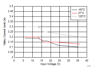
| ILS | Low-side switch current limit(6) | LM53603 | 3 | 3.6 | 4.3 | A |
| LM53602 | 2 | 2.4 | 2.8 | |||
| IZC | Zero-cross current limit | FPWM = 0 V | –0.02 | A | ||
| INEG | Negative current limit | FPWM = 3.3 V | –1.5 | A | ||
| Rdson | Power switch on-resistance | High-side MOSFET resistance | 135 | 290 | mΩ | |
| Low-side MOSFET resistance | 60 | 125 | ||||
| FSW | Switching frequency | VIN = 3.8 V to 18 V | 1.85 | 2.1 | 2.35 | MHz |
| VIN = 36 V | 1.2 | |||||
| FSYNC | Synchronizing frequency range | 1.9 | 2.1 | 2.3 | MHz | |
| VCC | Internal VCC voltage | VBIAS = 3.3 V | 3.15 | V | ||
| TSD | Thermal shutdown thresholds | Rising | 162 | 178 | °C | |
| Hysteresis, below | 18 | |||||
(1) Minimum and maximum limits are 100% production tested at 25°C. Limits over the operating temperature range are verified through correlation using Statistical Quality Control (SQC) methods. Limits are used to calculate Average Outgoing Quality Level (AOQL).
(2) This is the input voltage at which the device starts to operate (rising). The device shuts down when the input voltage goes below this value minus the hysteresis.
(3) This is the current used by the device, open loop. It does not represent the total input current of the system when in regulation. See Isupply in System Characteristics
(4) The FB pin is set to 5.5 V for this test.
(5) Below this voltage on the EN input, the device shuts down completely.
(6) See the Current Limit section for an explanation of valley current limit.
7.6 System Characteristics
The following specifications apply only to the typical application circuit, shown in Figure 15 with nominal component values. Typical values represent the most likely parametric norm at TJ = 25°C, and are provided for reference purposes only. The parameters in this table are not ensured.| PARAMETER | TEST CONDITIONS | MIN | TYP | MAX | UNIT | |
|---|---|---|---|---|---|---|
| VIN-MIN | Minimum input voltage for Vout to stay within ±2% of regulation(2) | VOUT = 3.3 V, IOUT = 3 A | 3.9 | V | ||
| VOUT = 3.3 V, IOUT = 1 A | 3.55 | |||||
| Regulation | Line Regulation | VOUT = 5 V, VIN = 8 V to 36 V, IOUT = 3 A | 7 | mV | ||
| VOUT = 3.3 V, VIN = 6 V to 36 V, IOUT = 3 A | 5 | |||||
| Load Regulation : Auto Mode | VOUT = 5 V, VIN = 12 V, IOUT = 10 µA to 3 A | 77 | mV | |||
| VOUT = 3.3 V, VIN = 12 V, IOUT = 10 µA to 3 A | 53 | |||||
| Load Regulation : FPWM Mode | VOUT = 5 V, VIN = 12 V, IOUT = 10 µA to 3 A | 12 | mV | |||
| VOUT = 3.3 V, VIN = 12 V, IOUT = 10 µA to 3 A | 9 | |||||
| ISUPPLY | Input supply current when in regulation(1) | VIN = 13.5 V, VOUT = 3.3 V, IOUT = 0 A | 24 | µA | ||
| VIN = 13.5 V, VOUT = 5 V, IOUT = 0 A | 34 | |||||
| VDROP | Dropout voltage (VIN – VOUT) | 5-V Option:
VOUT = 4.95 V, IOUT = 3 A, FSW < 1.85 MHz |
0.7 | V | ||
| 5-V Option:
VOUT = 5 V, IOUT = 3 A, FSW = 1.85 MHz |
1.8 | |||||
| 3.3-V Option:
VOUT = 3.27 V, IOUT = 3 A, FSW < 1.85 MHz |
0.65 | |||||
| 3.3-V Option:
VOUT = 3.3 V, IOUT = 3 A, FSW = 1.85 MHz |
1.8 | |||||
(1) Includes current into the EN pin, but does not include current due to the external resistive divider in adjustable output versions. See Input Supply Current section.
(2) This parameter is valid once the input voltage has risen above VIN-operate and the device has started up.
7.7 Timing Requirements
Limits apply to the recommended operating junction temperature range of –40°C to 150°C, unless otherwise noted. Minimum and maximum limits are verified through test, design, or statistical correlation. Typical values represent the most likely parametric norm at TJ = 25°C, and are provided for reference purposes only. Unless otherwise stated the following conditions apply: VIN = 13.5 V.| MIN | NOM | MAX | UNIT | ||
|---|---|---|---|---|---|
| TON | Minimum switch on-time, VIN = 20 V | 50 | 80 | ns | |
| TOFF | Minimum switch off-time, VIN = 3.8 V | 125 | 200 | ns | |
| TRESET-act | Delay time to RESET high signal | 2 | 3 | 4 | ms |
| TRESET-filter | Glitch filter time for RESET function | 12 | 25 | 45 | µs |
| TSS | Soft-start time | 1 | 2 | 3 | ms |
| TEN | Turnon delay, CVCC = 1 µF, TJ = 25°C(1) | 1 | ms | ||
| TW | Short-circuit wait time (Hiccup time) | 5.5 | ms | ||
(1) This is the time from the rising edge of EN to the time that the soft-start ramp begins.
7.8 Typical Characteristics
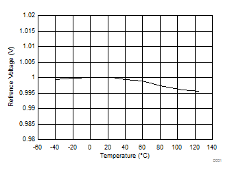
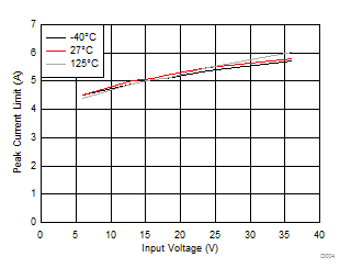
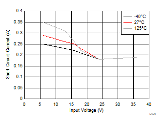
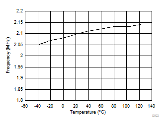
Unless otherwise specified the following conditions apply: VIN = 12 V, TA = 25°C. Specified temperatures are ambient.