JAJSDC5 June   2017 LM555-MIL

PRODUCTION DATA.  

  1. 特長
  2. アプリケーション
  3. 概要
  4. 改訂履歴
  5. Pin Configuration and Functions
  6. Specifications
    1. 6.1 Absolute Maximum Ratings
    2. 6.2 ESD Ratings
    3. 6.3 Recommended Operating Conditions
    4. 6.4 Thermal Information
    5. 6.5 Electrical Characteristics
    6. 6.6 Typical Characteristics
  7. Detailed Description
    1. 7.1 Overview
    2. 7.2 Functional Block Diagram
    3. 7.3 Feature Description
      1. 7.3.1 Direct Replacement for SE555/NE555
      2. 7.3.2 Timing From Microseconds Through Hours
      3. 7.3.3 Operates in Both Astable and Monostable Mode
    4. 7.4 Device Functional Modes
      1. 7.4.1 Monostable Operation
      2. 7.4.2 Astable Operation
  8. Application and Implementation
    1. 8.1 Application Information
    2. 8.2 Typical Application
      1. 8.2.1 Design Requirements
      2. 8.2.2 Detailed Design Procedure
        1. 8.2.2.1 Frequency Divider
        2. 8.2.2.2 Additional Information
      3. 8.2.3 Application Curves
  9. Power Supply Recommendations
  10. 10Layout
    1. 10.1 Layout Guidelines
    2. 10.2 Layout Example
  11. 11デバイスおよびドキュメントのサポート
    1. 11.1 ドキュメントの更新通知を受け取る方法
    2. 11.2 コミュニティ・リソース
    3. 11.3 商標
    4. 11.4 静電気放電に関する注意事項
    5. 11.5 Glossary
  12. 12メカニカル、パッケージ、および注文情報

パッケージ・オプション

メカニカル・データ(パッケージ|ピン)
  • YS|0
サーマルパッド・メカニカル・データ
発注情報

Layout

Layout Guidelines

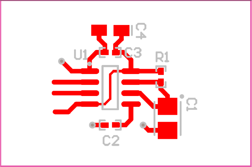
Standard PCB rules apply to routing the LM555-MIL. The 0.1-µF capacitor in parallel with a 1-µF electrolytic capacitor should be as close as possible to the LM555-MIL. The capacitor used for the time delay should also be placed as close to the discharge pin. A ground plane on the bottom layer can be used to provide better noise immunity and signal integrity.

Figure 20 is the basic layout for various applications.

  • C1 – based on time delay calculations
  • C2 – 0.01-µF bypass capacitor for control voltage pin
  • C3 – 0.1-µF bypass ceramic capacitor
  • C4 – 1-µF electrolytic bypass capacitor
  • R1 – based on time delay calculations
  • U1 – LMC555

Layout Example

LM555-MIL layoutex_snas548.gif Figure 20. Layout Example