JAJSF02F October 2008 – July 2019 LM5575-Q1
PRODUCTION DATA.
- 1 特長
- 2 アプリケーション
- 3 概要
- 4 改訂履歴
- 5 Pin Configuration and Functions
- 6 Specifications
- 7 Detailed Description
- 8 Application and Implementation
- 9 Power Supply Recommendations
- 10Layout
- 11デバイスおよびドキュメントのサポート
- 12メカニカル、パッケージ、および注文情報
パッケージ・オプション
メカニカル・データ(パッケージ|ピン)
- PWP|16
サーマルパッド・メカニカル・データ
- PWP|16
発注情報
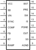
5 Pin Configuration and Functions
PWP Package
16-Pin HTSSOP With Exposed Thermal Pad
Top View

Pin Functions
| PIN | I/O | DESCRIPTION | APPLICATION INFORMATION | |
|---|---|---|---|---|
| NO. | NAME | |||
| 1 | VCC | O | Output of the bias regulator | VCC tracks VIN up to 9 V. Beyond 9 V, VCC is regulated to 7 V. A 0.1-µF to 1-µF ceramic decoupling capacitor is required. An external voltage (7.5 V – 14 V) can be applied to this pin to reduce internal power dissipation. |
| 2 | SD | I | Shutdown or UVLO input | If the SD pin voltage is lower than 0.7 V, the regulator is in a low power state. If the SD pin voltage is between 0.7 V and 1.225 V the regulator is in standby mode. If the SD pin voltage is higher than 1.225 V, the regulator is operational. An external voltage divider can be used to set a line undervoltage shutdown threshold. If the SD pin is left open circuit, a 5-µA pullup current source configures the regulator fully operational. |
| 3 | VIN | I | Input supply voltage | Nominal operating range: 6 V to 75 V. |
| 4 | SYNC | I | Oscillator synchronization input or output | The internal oscillator can be synchronized to an external clock with an external pulldown device. Multiple LM5575-Q1 devices can be synchronized together by connection of their SYNC pins. |
| 5 | COMP | O | Output of the internal error amplifier | The loop compensation network must be connected between this pin and the FB pin. |
| 6 | FB | I | Feedback signal from the regulated output | This pin is connected to the inverting input of the internal error amplifier. The regulation threshold is 1.225 V. |
| 7 | RT | I | Internal oscillator frequency set input | The internal oscillator is set with a single resistor connected between this pin and the AGND pin. |
| 8 | RAMP | O | Ramp control signal | An external capacitor connected between this pin and the AGND pin sets the ramp slope used for current mode control. Recommended capacitor range 50 pF to 2000 pF. |
| 9 | AGND | GND | Analog ground | Internal reference for the regulator control functions |
| 10 | SS | O | Soft start | An external capacitor and an internal 10-µA current source set the time constant for the rise of the error amp reference. The SS pin is held low during standby, VCC UVLO, and thermal shutdown. |
| 11 | OUT | O | Output voltage connection | Connect directly to the regulated output voltage. |
| 12 | PGND | GND | Power ground | Low-side reference for the PRE switch and the IS sense resistor. |
| 13 | IS | I | Current sense | Current measurement connection for the re-circulating diode. An internal sense resistor and a sample and hold circuit sense the diode current near the conclusion of the off-time. This current measurement provides the DC level of the emulated current ramp. |
| 14 | SW | O | Switching node | The source terminal of the internal buck switch. Connect the SW pin to the external Schottky diode and to the buck inductor. |
| 15 | PRE | O | Pre-charge assist for the bootstrap capacitor | This open-drain output can be connected to SW pin to help charging the bootstrap capacitor during very light load conditions or in applications where the output may be pre-charged before the LM5575-Q1 is enabled. An internal pre-charge MOSFET is turned on for 250 ns each cycle just prior to the on-time interval of the buck switch. |
| 16 | BST | I | Boost input for bootstrap capacitor | An external capacitor is required between the BST and the SW pins. TI recommends a 0.022-µF ceramic capacitor. The capacitor is charged from VCC through an internal diode during the off-time of the buck switch. |
| NA | EP | -- | Exposed Pad | Exposed metal pad on the underside of the device. TI recommends to connect this pad to the PWB ground plane to help with heat dissipation. |