JAJSIR9C March 2020 – June 2021 LM61440-Q1
PRODUCTION DATA
- 1 特長
- 2 アプリケーション
- 3 概要
- 4 Revision History
- 5 Description (continued)
- 6 Device Comparison Table
- 7 Pin Configuration and Functions
- 8 Specifications
-
9 Detailed Description
- 9.1 Overview
- 9.2 Functional Block Diagram
- 9.3
Feature Description
- 9.3.1 EN/SYNC Uses for Enable and VIN UVLO
- 9.3.2 EN/SYNC Pin Uses for Synchronization
- 9.3.3 Clock Locking
- 9.3.4 Adjustable Switching Frequency
- 9.3.5 PGOOD Output Operation
- 9.3.6 Internal LDO, VCC UVLO, and BIAS Input
- 9.3.7 Bootstrap Voltage and VCBOOT-UVLO (CBOOT Pin)
- 9.3.8 Adjustable SW Node Slew Rate
- 9.3.9 Spread Spectrum
- 9.3.10 Soft Start and Recovery From Dropout
- 9.3.11 Output Voltage Setting
- 9.3.12 Overcurrent and Short Circuit Protection
- 9.3.13 Thermal Shutdown
- 9.3.14 Input Supply Current
- 9.4 Device Functional Modes
-
10Application and Implementation
- 10.1 Application Information
- 10.2
Typical Application
- 10.2.1 Design Requirements
- 10.2.2
Detailed Design Procedure
- 10.2.2.1 Choosing the Switching Frequency
- 10.2.2.2 Setting the Output Voltage
- 10.2.2.3 Inductor Selection
- 10.2.2.4 Output Capacitor Selection
- 10.2.2.5 Input Capacitor Selection
- 10.2.2.6 BOOT Capacitor
- 10.2.2.7 BOOT Resistor
- 10.2.2.8 VCC
- 10.2.2.9 BIAS
- 10.2.2.10 CFF and RFF Selection
- 10.2.2.11 External UVLO
- 10.2.3 Application Curves
- 11Power Supply Recommendations
- 12Layout
- 13Device and Documentation Support
- 14Mechanical, Packaging, and Orderable Information
9.4.3.2.1 Diode Emulation
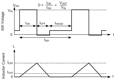
Diode emulation prevents reverse current through the inductor which requires a lower frequency needed to regulate given a fixed peak inductor current. Diode emulation also limits ripple current as frequency is reduced. With a fixed peak current, as output current is reduced to zero, frequency must be reduced to near zero to maintain regulation.

In auto mode, the low-side device is turned off once SW node current is near zero. As a result, once output current is less than half of what inductor ripple would be in CCM, the part operates in DCM which is equivalent to the statement that diode emulation is active.
Figure 9-16 PFM OperationThe LM61440-Q1 has a minimum peak inductor current setting while in auto mode. Once current is reduced to a low value with fixed input voltage, on-time is constant. Regulation is then achieved by adjusting frequency. This mode of operation is called PFM mode regulation.