JAJSIO7D May   2019  – July 2022 LM61460

PRODUCTION DATA  

  1. 特長
  2. アプリケーション
  3. 概要
  4. Revision History
  5. Device Comparison Table
  6. Pin Configuration and Functions
  7. Specifications
    1. 7.1 Absolute Maximum Ratings
    2.     ESD Ratings
    3. 7.2 Recommended Operating Conditions
    4. 7.3 Thermal Information
    5. 7.4 Electrical Characteristics
    6. 7.5 Timing Characteristics
    7. 7.6 Systems Characteristics
    8. 7.7 Typical Characteristics
  8. Detailed Description
    1. 8.1 Overview
    2. 8.2 Functional Block Diagram
    3. 8.3 Feature Description
      1. 8.3.1  EN/SYNC Uses for Enable and VIN UVLO
      2. 8.3.2  EN/SYNC Pin Uses for Synchronization
      3. 8.3.3  Clock Locking
      4. 8.3.4  Adjustable Switching Frequency
      5. 8.3.5  PGOOD Output Operation
      6. 8.3.6  Internal LDO, VCC UVLO, and BIAS Input
      7. 8.3.7  Bootstrap Voltage and VCBOOT-UVLO (CBOOT Pin)
      8. 8.3.8  Adjustable SW Node Slew Rate
      9. 8.3.9  Spread Spectrum
      10. 8.3.10 Soft Start and Recovery From Dropout
      11. 8.3.11 Output Voltage Setting
      12. 8.3.12 Overcurrent and Short Circuit Protection
      13. 8.3.13 Thermal Shutdown
      14. 8.3.14 Input Supply Current
    4. 8.4 Device Functional Modes
      1. 8.4.1 Shutdown Mode
      2. 8.4.2 Standby Mode
      3. 8.4.3 Active Mode
        1. 8.4.3.1 CCM Mode
        2. 8.4.3.2 Auto Mode – Light-Load Operation
          1. 8.4.3.2.1 Diode Emulation
          2. 8.4.3.2.2 Frequency Reduction
        3. 8.4.3.3 FPWM Mode – Light-Load Operation
        4. 8.4.3.4 Minimum On-Time (High Input Voltage) Operation
        5. 8.4.3.5 Dropout
  9. Application and Implementation
    1. 9.1 Application Information
    2. 9.2 Typical Application
      1. 9.2.1 Design Requirements
      2. 9.2.2 Detailed Design Procedure
        1. 9.2.2.1  Choosing the Switching Frequency
        2. 9.2.2.2  Setting the Output Voltage
        3. 9.2.2.3  Inductor Selection
        4. 9.2.2.4  Output Capacitor Selection
        5. 9.2.2.5  Input Capacitor Selection
        6. 9.2.2.6  BOOT Capacitor
        7. 9.2.2.7  BOOT Resistor
        8. 9.2.2.8  VCC
        9. 9.2.2.9  BIAS
        10. 9.2.2.10 CFF and RFF Selection
        11. 9.2.2.11 External UVLO
      3. 9.2.3 Application Curves
      4. 9.2.4 USB Type-C System Example
        1. 9.2.4.1 Design Requirements
        2. 9.2.4.2 Detailed Design Procedure
        3. 9.2.4.3 Application Curves
  10. 10Power Supply Recommendations
  11. 11Layout
    1. 11.1 Layout Guidelines
      1. 11.1.1 Ground and Thermal Considerations
    2. 11.2 Layout Example
  12. 12Device and Documentation Support
    1. 12.1 Documentation Support
      1. 12.1.1 Related Documentation
    2. 12.2 Receiving Notification of Documentation Updates
    3. 12.3 サポート・リソース
    4. 12.4 Trademarks
    5. 12.5 Electrostatic Discharge Caution
    6. 12.6 Glossary
  13. 13Mechanical, Packaging, and Orderable Information

パッケージ・オプション

メカニカル・データ(パッケージ|ピン)
サーマルパッド・メカニカル・データ
発注情報

Adjustable Switching Frequency

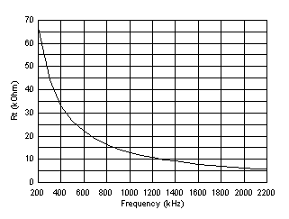
A resistor tied from the device RT pin to AGND is used to set operating frequency. Use Equation 2 or refer to Figure 8-5 for resistor values. Note that a resistor value outside of the recommended range can cause the device to shut down. This prevents unintended operation if RT pin is shorted to ground or left open. Do not apply a pulsed signal to this pin to force synchronization. If synchronization is needed, refer to Section 8.3.2.

Equation 2. RRT(kΩ) = (1 / fSW(kHz) - 3.3 x 10-5) × 1.346 x 104
GUID-A07A5EF7-A62B-4605-83DF-67FC371E8573-low.gif Figure 8-5 Setting Clock Frequency