JAJSJT2D February 2020 – August 2021 LM61480-Q1 , LM61495-Q1 , LM62460-Q1
PRODUCTION DATA
- 1 特長
- 2 アプリケーション
- 3 概要
- 4 Revision History
- 5 Device Comparison Table
- 6 Pin Configuration and Functions
- 7 Specifications
-
8 Detailed Description
- 8.1 Overview
- 8.2 Functional Block Diagram
- 8.3
Feature Description
- 8.3.1 Output Voltage Selection
- 8.3.2 Enable EN Pin and Use as VIN UVLO
- 8.3.3 SYNC/MODE Uses for Synchronization
- 8.3.4 Clock Locking
- 8.3.5 Adjustable Switching Frequency
- 8.3.6 RESET Output Operation
- 8.3.7 Internal LDO, VCC UVLO, and BIAS Input
- 8.3.8 Bootstrap Voltage and VCBOOT-UVLO (CBOOT Pin)
- 8.3.9 Adjustable SW Node Slew Rate
- 8.3.10 Spread Spectrum
- 8.3.11 Soft Start and Recovery From Dropout
- 8.3.12 Overcurrent and Short Circuit Protection
- 8.3.13 Hiccup
- 8.3.14 Thermal Shutdown
- 8.4 Device Functional Modes
-
9 Application and Implementation
- 9.1 Application Information
- 9.2
Typical Application
- 9.2.1 Design Requirements
- 9.2.2
Detailed Design Procedure
- 9.2.2.1 Choosing the Switching Frequency
- 9.2.2.2 Setting the Output Voltage
- 9.2.2.3 Inductor Selection
- 9.2.2.4 Output Capacitor Selection
- 9.2.2.5 Input Capacitor Selection
- 9.2.2.6 BOOT Capacitor
- 9.2.2.7 BOOT Resistor
- 9.2.2.8 VCC
- 9.2.2.9 CFF and RFF Selection
- 9.2.2.10 RSPSP Selection
- 9.2.2.11 RT Selection
- 9.2.2.12 RMODE Selection
- 9.2.2.13 External UVLO
- 9.2.2.14 Maximum Ambient Temperature
- 9.2.3 Application Curves
- 10Power Supply Recommendations
- 11Layout
- 12Device and Documentation Support
- 13Mechanical, Packaging, and Orderable Information
パッケージ・オプション
メカニカル・データ(パッケージ|ピン)
- RPH|16
サーマルパッド・メカニカル・データ
- RPH|16
発注情報
8.3.11 Soft Start and Recovery From Dropout
When designing with the LM6x4xx-Q1, slowed rise in output voltage due to recovery from dropout and soft start must be considered separate phenomena. Soft start is triggered by any of the following conditions:
- EN is used to turn on the device.
- Recovery from a hiccup waiting period; see Section 8.3.13.
- Recovery from shutdown due to overtemperature protection
- Power is applied to the VIN of the IC or the VCC UVLO is released.
Once soft start is triggered, the IC takes the following actions:
- The reference used by the IC to regulate output voltage is slowly ramped from zero. The net result is that output voltage, if previously 0 V, takes tSS to reach 90% of its desired value.
- Operating mode is set to auto, activating diode emulation. This allows start-up without pulling output low if there is a voltage already present on the output.
- Hiccup is disabled for the duration of soft start; see Section 8.3.13.
All of these actions together provide start-up with limited inrush currents. They also allow the use of output capacitors and loading conditions that cause current to border on current limit during start-up without triggering hiccup. In addition, if output voltage is already present, output is not pulled down. See Figure 8-13.

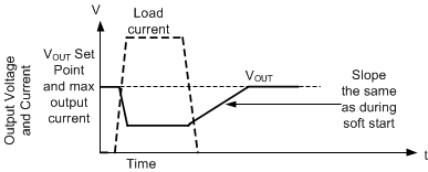
Any time output voltage is more than a few percent low for any reason, output voltage ramps up slowly. This condition, called recovery from dropout, differs from soft start in three important ways:
- Hiccup is allowed only if output voltage is less than 0.4 times its set point. Note that during dropout regulation itself, hiccup is inhibited. See Section 8.3.13.
- FPWM mode is allowed during recovery from dropout. If output voltage were to suddenly be pulled up by an external supply, the LM6x4xx-Q1 can pull down on the output. Note that all the protections that are present during normal operation are in place, protecting the device if output is shorted to a high voltage or ground.
- The reference voltage is set to approximately 1% above that needed to achieve the current output voltage. It is not started from zero.
Despite the name, recovery from dropout is active whenever output voltage is more than a few percent lower than the setpoint for long enough that:
- Duty factor is controlled by minimum on-time or
- When the part is operating in current limit.
- Dropout: When there is insufficient input voltage for the desired output voltage to be generated. See Section 8.4.3.5.
- Overcurrent that is not severe enough to trigger hiccup or if the duration is too short to trigger hiccup. See Section 8.3.13.
