JAJSJT2D February 2020 – August 2021 LM61480-Q1 , LM61495-Q1 , LM62460-Q1
PRODUCTION DATA
- 1 特長
- 2 アプリケーション
- 3 概要
- 4 Revision History
- 5 Device Comparison Table
- 6 Pin Configuration and Functions
- 7 Specifications
-
8 Detailed Description
- 8.1 Overview
- 8.2 Functional Block Diagram
- 8.3
Feature Description
- 8.3.1 Output Voltage Selection
- 8.3.2 Enable EN Pin and Use as VIN UVLO
- 8.3.3 SYNC/MODE Uses for Synchronization
- 8.3.4 Clock Locking
- 8.3.5 Adjustable Switching Frequency
- 8.3.6 RESET Output Operation
- 8.3.7 Internal LDO, VCC UVLO, and BIAS Input
- 8.3.8 Bootstrap Voltage and VCBOOT-UVLO (CBOOT Pin)
- 8.3.9 Adjustable SW Node Slew Rate
- 8.3.10 Spread Spectrum
- 8.3.11 Soft Start and Recovery From Dropout
- 8.3.12 Overcurrent and Short Circuit Protection
- 8.3.13 Hiccup
- 8.3.14 Thermal Shutdown
- 8.4 Device Functional Modes
-
9 Application and Implementation
- 9.1 Application Information
- 9.2
Typical Application
- 9.2.1 Design Requirements
- 9.2.2
Detailed Design Procedure
- 9.2.2.1 Choosing the Switching Frequency
- 9.2.2.2 Setting the Output Voltage
- 9.2.2.3 Inductor Selection
- 9.2.2.4 Output Capacitor Selection
- 9.2.2.5 Input Capacitor Selection
- 9.2.2.6 BOOT Capacitor
- 9.2.2.7 BOOT Resistor
- 9.2.2.8 VCC
- 9.2.2.9 CFF and RFF Selection
- 9.2.2.10 RSPSP Selection
- 9.2.2.11 RT Selection
- 9.2.2.12 RMODE Selection
- 9.2.2.13 External UVLO
- 9.2.2.14 Maximum Ambient Temperature
- 9.2.3 Application Curves
- 10Power Supply Recommendations
- 11Layout
- 12Device and Documentation Support
- 13Mechanical, Packaging, and Orderable Information
パッケージ・オプション
メカニカル・データ(パッケージ|ピン)
- RPH|16
サーマルパッド・メカニカル・データ
- RPH|16
発注情報
8.3.6 RESET Output Operation
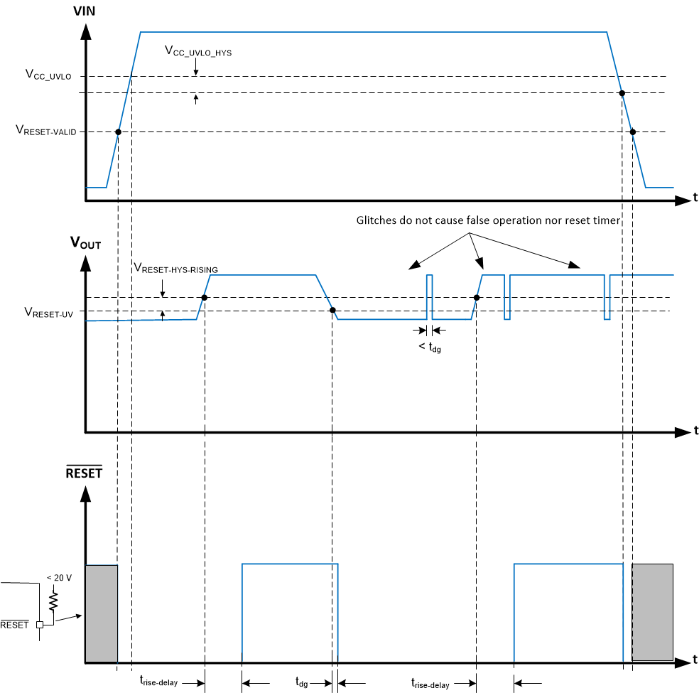
While the RESET function of the LM6x4xx-Q1 resembles a standard power-good function, the functionality is designed to replace a discrete reset IC, reducing BOM cost. There are three major differences between the reset function and the normal power-good function seen in most regulators:
- A delay has been added for release of reset. See Table 8-1.
- RESET output signals a fault (pulls its output to ground) while the part is disabled.
- RESET continues to operate with input voltage as low as 1.2 V. Below this input voltage, RESET output can be high impedance.
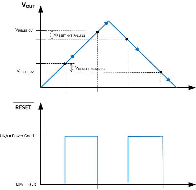
 Figure 8-7 RESET Static Voltage Thresholds
 Figure 8-8 RESET Timing Diagram (Excludes OV Events)
| FAULT CONDITION INITIATED | FAULT CONDITION ENDS (AFTER WHICH tRESET_ACT MUST PASS BEFORE RESET OUTPUT IS RELEASED) |
|---|---|
| FB below VRESET_UV for longer than tRESET_FILTER | FB above VRESET_UV + VRESET_HYST for longer than tRESET_FILTER |
| FB above VRESET_OV for longer than tRESET_FILTER | FB below VRESET_OV - VRESET_HYST for longer than tRESET_FILTER |
| Junction temperature exceeds TSD_R | Junction temperature falls below TSD_F(1) |
| EN low | tEN passes after EN becomes high(1) |
| VIN falls low enough so that VCC falls below VCC_UVLO - VCC_UVLO_HYST. This value is called VIN_OPERATE. | Voltage on VIN is high enough so that VCC pin exceed VCC_UVLO(1) |
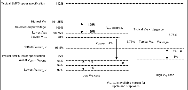
The threshold voltage for the RESET function is specified to take advantage of the availability of the LM6x4xx-Q1 internal feedback threshold to the RESET circuit. This allows a maximum threshold of 96.5% of selected output voltage to be specified at the same time as 96% of actual operating point. The net result is a more accurate reset function while expanding the system allowance for transient response. See the output voltage error stack-up comparison in Figure 8-9.
In addition to signaling a fault upon overvoltage detection (FB above VRESET_OV), the switch node is shut down and a small, approximately 1-mA pulldown is applied to the SW node.
 Figure 8-9 Reset Threshold Voltage Stack-up