JAJSMA0A July   2020  – July 2021 LM63610-Q1

PRODUCTION DATA  

  1. 特長
  2. アプリケーション
  3. 概要
  4. Revision History
  5. Device Comparison Table
  6. Pin Configuration and Functions
  7. Specifications
    1. 7.1 Absolute Maximum Ratings
    2. 7.2 ESD Ratings
    3. 7.3 Recommended Operating Conditions
    4. 7.4 Thermal Information
    5. 7.5 Electrical Characteristics
    6. 7.6 Timing Characteristics
    7. 7.7 Switching Characteristics
    8. 7.8 System Characteristics
    9. 7.9 Typical Characteristics
  8. Detailed Description
    1. 8.1 Overview
    2. 8.2 Functional Block Diagram
    3. 8.3 Feature Description
      1. 8.3.1 Sync/Mode Selection
      2. 8.3.2 Output Voltage Selection
      3. 8.3.3 Switching Frequency Selection
        1. 8.3.3.1 Spread Spectrum Option
      4. 8.3.4 Enable and Start-up
      5. 8.3.5 RESET Flag Output
      6. 8.3.6 Undervoltage Lockout and Thermal Shutdown and Output Discharge
    4. 8.4 Device Functional Modes
      1. 8.4.1 Overview
      2. 8.4.2 Light Load Operation
        1. 8.4.2.1 Sync/FPWM Operation
      3. 8.4.3 Dropout Operation
      4. 8.4.4 Minimum On-time Operation
      5. 8.4.5 Current Limit and Short-Circuit Operation
  9. Application and Implementation
    1. 9.1 Application Information
    2. 9.2 Typical Application
      1. 9.2.1 Design Requirements
      2. 9.2.2 Detailed Design Procedure
        1. 9.2.2.1 Choosing the Switching Frequency
        2. 9.2.2.2 Setting the Output Voltage
          1. 9.2.2.2.1 CFF Selection
        3. 9.2.2.3 Inductor Selection
        4. 9.2.2.4 Output Capacitor Selection
        5. 9.2.2.5 Input Capacitor Selection
        6. 9.2.2.6 CBOOT
        7. 9.2.2.7 VCC
        8. 9.2.2.8 External UVLO
        9. 9.2.2.9 Maximum Ambient Temperature
      3. 9.2.3 Application Curves
      4. 9.2.4 EMI Performance Curves
    3. 9.3 What to Do and What Not to Do
  10. 10Power Supply Recommendations
  11. 11Layout
    1. 11.1 Layout Guidelines
      1. 11.1.1 Ground and Thermal Considerations
    2. 11.2 Layout Example
  12. 12Device and Documentation Support
    1. 12.1 Documentation Support
      1. 12.1.1 Related Documentation
    2. 12.2 Receiving Notification of Documentation Updates
    3. 12.3 サポート・リソース
    4. 12.4 Trademarks
    5. 12.5 Electrostatic Discharge Caution
    6. 12.6 Glossary
  13. 13Mechanical, Packaging, and Orderable Information

パッケージ・オプション

メカニカル・データ(パッケージ|ピン)
サーマルパッド・メカニカル・データ
発注情報

Application Curves

Unless otherwise specified, the following conditions apply: VIN = 13.5 V, TA = 25°C. shows the circuit with the appropriate BOM from .
Unless otherwise specified, the following conditions apply: VIN = 13.5 V, TA = 25°C. shows the circuit with the appropriate BOM from .GUID-4FA47337-3158-440A-B76D-44684318B3E6-low.gif
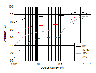
LM63610 VOUT = 5 V ƒSW = 400 kHz (AUTO)
Figure 9-5 Efficiency. Unless otherwise specified, the following conditions apply: VIN = 13.5 V, TA = 25°C. shows the circuit with the appropriate BOM from .
GUID-C9B28EB6-BA41-4E83-B20F-BD1A244A2F99-low.gif
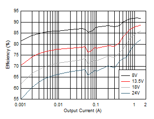
LM63610 VOUT = 3.3 V ƒSW = 400 kHz (AUTO)
Figure 9-7 Efficiency
GUID-2C760828-18B3-483D-AADE-BBC9F76193A0-low.gif
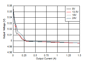
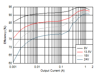
LM63610VOUT = 5 VƒSW = 2100 kHz (AUTO)
Figure 9-9 Line and Load Regulation
GUID-59AC0B06-055B-4F24-8D71-E4A1F2B73A60-low.gif
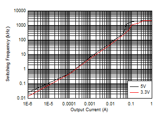
LM63610 VIN = 13.5 V ƒSW = 2100 kHz (AUTO)
Figure 9-11 Switching Frequency versus Output Current
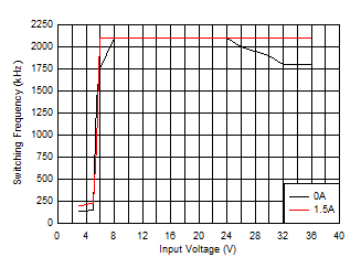
GUID-EA3E6F0D-070F-46ED-9144-A9FDDD428686-low.gif
LM63610 VOUT = 5 V ƒSW = 2100 kHz (FPWM)
Figure 9-13 Switching Frequency versus Input Voltage
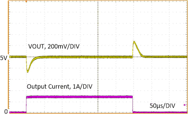
GUID-FE03B6C8-06D6-4636-8B4C-57847E60B959-low.gif
LM63610 VOUT = 5 V ƒSW = 2100 kHz
0 A to 1.5 A, 2µs FPWM
Figure 9-15 Load Transient
GUID-70843760-F3C2-4FC1-8F81-3AEECA4DD280-low.gif
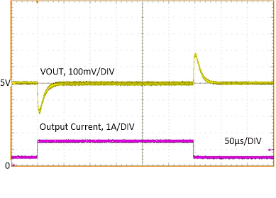
LM63610 VOUT = 5 V ƒSW = 2100 kHz
0.5 A to 1.5 A, 2µs AUTO
Figure 9-17 Load Transient
GUID-9AA17BDD-115A-48E9-BFB0-3D1DB0BABFAE-low.gif
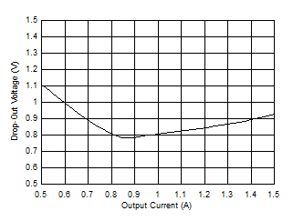
LM63610 ƒSW = 1850 kHz (AUTO)
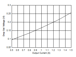
Figure 9-19 Dropout Voltage versus Output Current to 1.85 MHz
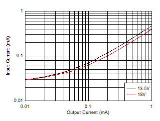
GUID-B2F684AE-D830-4CFA-BFC1-023CE84A4FDE-low.gif
LM63610 VOUT = 5 V ƒSW = 2100 kHz (AUTO)
Figure 9-21 Input Supply Current versus Output Current
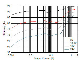
GUID-D7EAB54E-7BD0-4417-B976-CFB61193BBFB-low.gif
LM63610 VOUT = 5 V ƒSW = 2100 kHz (AUTO)
Figure 9-6 Efficiency
GUID-8CCC9D1D-A3AB-475B-AB2E-7720A85C3BB7-low.gif
LM63610 VOUT = 3.3 V ƒSW = 2100 kHz (AUTO)
Figure 9-8 Efficiency
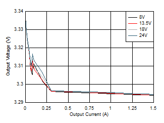
GUID-D33974F8-AD60-4C10-AA9F-27D28C8C3AEF-low.gif
LM63610VOUT = 3.3 VƒSW = 2100 kHz (AUTO)
Figure 9-10 Line and Load Regulation
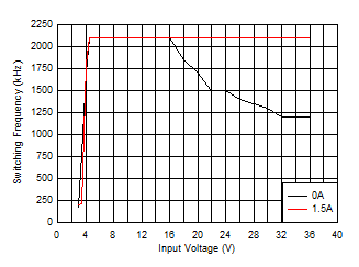
GUID-066E83E9-E37E-4FEE-9311-2EBFFBC875FE-low.gif
LM63610 VOUT = 3.3 V ƒSW = 2100 kHz (FPWM)
Figure 9-12 Switching Frequency versus Input Voltage
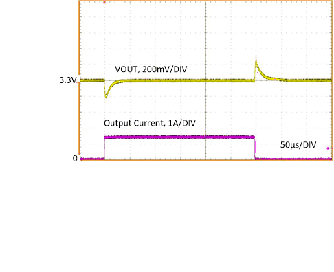
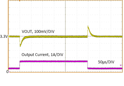
GUID-7C3EC3A8-E270-424B-8897-07A387918F96-low.gif
LM63610 VOUT = 3.3 V ƒSW = 2100 kHz
0 A to 1.5 A, 2µs FPWM
Figure 9-14 Load Transient
GUID-8044F6B9-1A7F-4C52-8A49-18CBBDAE5F8C-low.gif
LM63610 VOUT = 3.3 V ƒSW = 2100 kHz
0.5 A to 1.5 A, 2µs AUTO
Figure 9-16 Load Transient
GUID-008A8546-5E57-4205-9E2C-96260B25B5CC-low.gif
LM63610 ƒSW = 140 kHz (AUTO)
Figure 9-18 Dropout Voltage versus Output Current for -1% Drop
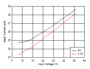
GUID-E17BFD36-745B-46FE-922F-E473EC06A9DB-low.gif
LM63610 IOUT = 0 A ƒSW = 2100 kHz (AUTO)
Figure 9-20 Input Supply Current versus Input Voltage
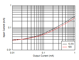
GUID-BB8EFAA4-7580-4020-A415-04C5F93D4A8D-low.gif
LM63610 VOUT = 3.3 V ƒSW = 2100 kHz (AUTO)
Figure 9-22 Input Supply Current versus Output Current
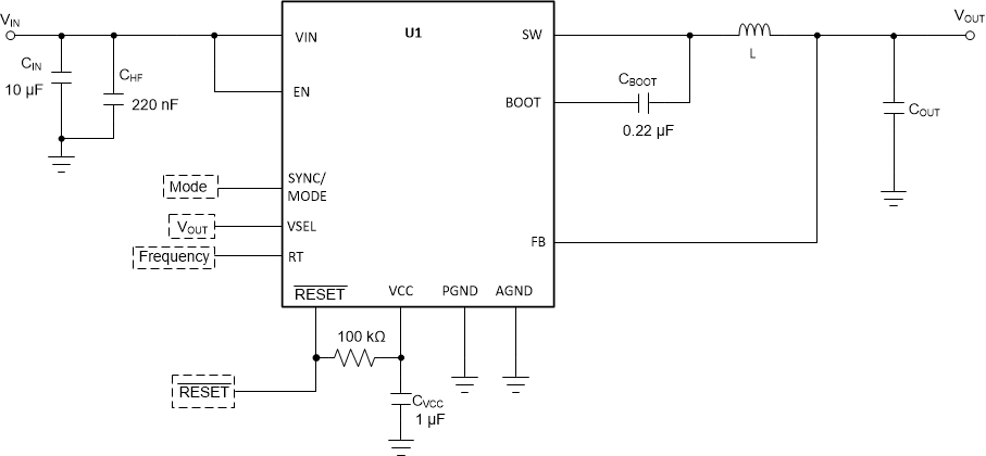
GUID-B0801334-3F79-40FB-9D50-7DD7F0BC5470-low.gif Figure 9-23 Circuit for Typical Application Curves
Table 9-3 BOM for Typical Application Curves
VOUT(1) FREQUENCY OUTPUT CURRENT COUT L U1
3.3 V 400 kHz 1 A 2 × 22 µF 10 µH, 40 mΩ LM63610
3.3 V 2100 kHz 1 A 1 × 10 µF 4.7 µH, 30 mΩ LM63610
5 V 400 kHz 1 A 2 × 22 µF 10 µH, 40 mΩ LM63610
5 V 2100 kHz 1 A 1 × 10 µF 4.7 µH, 30 mΩ LM63610
The values in this table were selected to enhance certain performance criteria and may not represent typical values.