JAJSMA0A July   2020  – July 2021 LM63610-Q1

PRODUCTION DATA  

  1. 特長
  2. アプリケーション
  3. 概要
  4. Revision History
  5. Device Comparison Table
  6. Pin Configuration and Functions
  7. Specifications
    1. 7.1 Absolute Maximum Ratings
    2. 7.2 ESD Ratings
    3. 7.3 Recommended Operating Conditions
    4. 7.4 Thermal Information
    5. 7.5 Electrical Characteristics
    6. 7.6 Timing Characteristics
    7. 7.7 Switching Characteristics
    8. 7.8 System Characteristics
    9. 7.9 Typical Characteristics
  8. Detailed Description
    1. 8.1 Overview
    2. 8.2 Functional Block Diagram
    3. 8.3 Feature Description
      1. 8.3.1 Sync/Mode Selection
      2. 8.3.2 Output Voltage Selection
      3. 8.3.3 Switching Frequency Selection
        1. 8.3.3.1 Spread Spectrum Option
      4. 8.3.4 Enable and Start-up
      5. 8.3.5 RESET Flag Output
      6. 8.3.6 Undervoltage Lockout and Thermal Shutdown and Output Discharge
    4. 8.4 Device Functional Modes
      1. 8.4.1 Overview
      2. 8.4.2 Light Load Operation
        1. 8.4.2.1 Sync/FPWM Operation
      3. 8.4.3 Dropout Operation
      4. 8.4.4 Minimum On-time Operation
      5. 8.4.5 Current Limit and Short-Circuit Operation
  9. Application and Implementation
    1. 9.1 Application Information
    2. 9.2 Typical Application
      1. 9.2.1 Design Requirements
      2. 9.2.2 Detailed Design Procedure
        1. 9.2.2.1 Choosing the Switching Frequency
        2. 9.2.2.2 Setting the Output Voltage
          1. 9.2.2.2.1 CFF Selection
        3. 9.2.2.3 Inductor Selection
        4. 9.2.2.4 Output Capacitor Selection
        5. 9.2.2.5 Input Capacitor Selection
        6. 9.2.2.6 CBOOT
        7. 9.2.2.7 VCC
        8. 9.2.2.8 External UVLO
        9. 9.2.2.9 Maximum Ambient Temperature
      3. 9.2.3 Application Curves
      4. 9.2.4 EMI Performance Curves
    3. 9.3 What to Do and What Not to Do
  10. 10Power Supply Recommendations
  11. 11Layout
    1. 11.1 Layout Guidelines
      1. 11.1.1 Ground and Thermal Considerations
    2. 11.2 Layout Example
  12. 12Device and Documentation Support
    1. 12.1 Documentation Support
      1. 12.1.1 Related Documentation
    2. 12.2 Receiving Notification of Documentation Updates
    3. 12.3 サポート・リソース
    4. 12.4 Trademarks
    5. 12.5 Electrostatic Discharge Caution
    6. 12.6 Glossary
  13. 13Mechanical, Packaging, and Orderable Information

パッケージ・オプション

メカニカル・データ(パッケージ|ピン)
サーマルパッド・メカニカル・データ
発注情報

Typical Application

Figure 9-1 shows a typical application circuit for the device. This device is designed to function over a wide range of external components and system parameters. However, the internal compensation is optimized for a certain range of external inductance and output capacitance. As a quick start guide, see for typical component values.
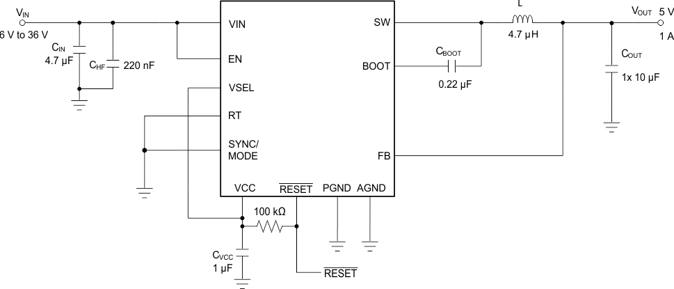
GUID-84DCF761-2E8E-4635-8F29-3CFA6DED9FEB-low.gif Figure 9-1 Example Application Circuit VIN = 12 V, VOUT = 5 V, IOUT = 1 A, ƒSW = 2.1 MHz
Table 9-1 Typical External Component Values for 1 A Output Current
ƒSW (kHz)VOUTL (µH)(1)TYPICAL(2) COUTMINIMUM(2) COUTVSELRTCINCBOOTCVCC
4003.3104 × 10 µF2 × 10 µFAGNDVCC4.7 µF + 220 nF220 nF1 µF
21003.34.72 × 10 µF1 × 10 µFAGNDAGND4.7 µF + 220 nF220 nF1 µF
4005104 × 10 µF2 × 10 µFVCCVCC4.7 µF + 220 nF220 nF1 µF
210054.72 × 10 µF1 × 10 µFVCCAGND4.7 µF + 220 nF220 nF1 µF
See the Inductor Selection section.
See the Output Capacitor Selection section.