JAJSMA0A July 2020 – July 2021 LM63610-Q1
PRODUCTION DATA
- 1 特長
- 2 アプリケーション
- 3 概要
- 4 Revision History
- 5 Device Comparison Table
- 6 Pin Configuration and Functions
- 7 Specifications
- 8 Detailed Description
- 9 Application and Implementation
- 10Power Supply Recommendations
- 11Layout
- 12Device and Documentation Support
- 13Mechanical, Packaging, and Orderable Information
パッケージ・オプション
メカニカル・データ(パッケージ|ピン)
サーマルパッド・メカニカル・データ
発注情報
8.4.5 Current Limit and Short-Circuit Operation
The LM63610-Q1 incorporates both peak and valley inductor current limits to provide protection to the device from overloads and short circuits and limit the maximum output current. Valley current limit prevents inductor current run-away during short circuits on the output, while both peak and valley limits work together to limit the maximum output current of the converter. A "hiccup" type mode is also incorporated for sustained short circuits. Finally, a zero current detector is used on the low-side power MOSFET to implement DEM at light loads (see the Glossary). The nominal value of this limit is about 0 A.
As the device is overloaded, a point is reached where the valley of the inductor current cannot reach below ILS-LIMIT before the next clock cycle. When this occurs, the valley current limit control skips that cycle, causing the switching frequency to drop. Further overload causes the switching frequency to continue to drop, but the output voltage remains in regulation. As the overload is increased, both the inductor current ripple and peak current increases until the high-side current limit, ISC, is reached. When this limit is activated, the switch duty cycle is reduced and the output voltage falls out of regulation. This represents the maximum output current from the converter and is given approximately by Equation 3. The output voltage and switching frequency continue to drop as the device moves deeper into overload while the output current remains at approximately IOMAX.

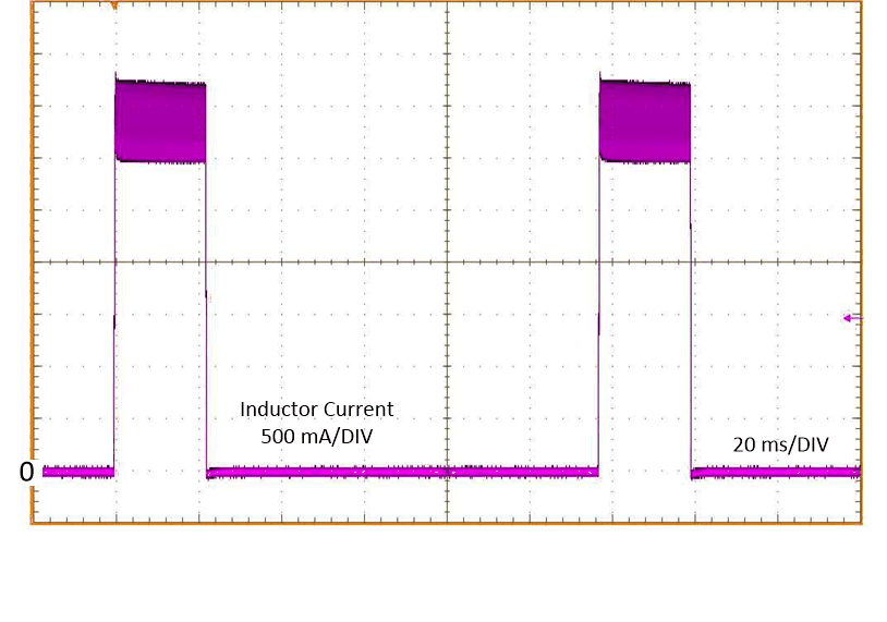
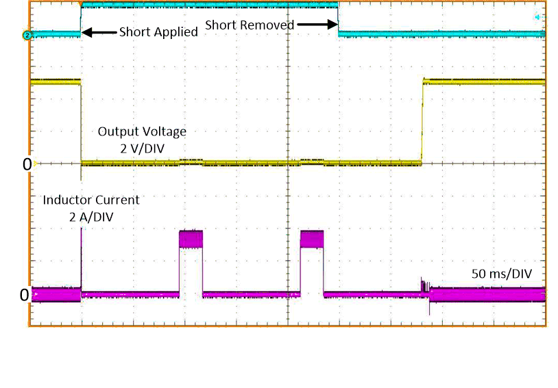
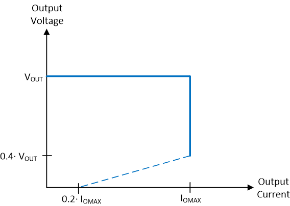
If a severe overload or short circuit causes the FB voltage to fall below VHICCUP, the convert enters "hiccup" mode. VHICCUP represents about 40% of the nominal programmed output voltage. In this mode, the device stops switching for tOC, or about 100 ms and then goes through a normal restart with soft start. If the short-circuit condition remains, the device runs in current limit for a little longer than tOC_active, or about 23 ms, and then shuts down again. This cycle repeats, as shown in Figure 8-10 as long as the short-circuit condition persists. This mode of operation reduces the temperature rise of the device during a sustained short on the output. The output current in this mode is approximately 20% of IOMAX. Once the output short is removed and the tOC delay is passed, the output voltage recovers normally as shown in Figure 8-11.
See Figure 8-12 for the overall output voltage versus output current characteristic.
 Figure 8-10 Inductor Current Burst in Short-Circuit Mode; Refer to LM63615/25 Data
Sheet
 Figure 8-11 Short-Circuit Transient and Recovery; Refer to LM63615/25 Data
Sheet
 Figure 8-12 Output Voltage versus Output Current in Current Limit