JAJSIE0F November 2019 – September 2024 LM63635-Q1
PRODUCTION DATA
- 1
- 1 特長
- 2 アプリケーション
- 3 概要
- 4 Device Comparison Table
- 5 Pin Configuration and Functions
- 6 Specifications
- 7 Detailed Description
- 8 Application and Implementation
- 9 Device and Documentation Support
- 10Revision History
- 11Mechanical, Packaging, and Orderable Information
パッケージ・オプション
メカニカル・データ(パッケージ|ピン)
サーマルパッド・メカニカル・データ
発注情報
7.4.1 Overview
In typical usage, the device is put in AUTO mode (SYNC/MODE pin = ground). In AUTO mode, the device moves between PWM and PFM as the load changes. At light loads, the regulator operates in PFM where the switching frequency is varied to regulate the output voltage. At higher loads, the mode changes to PWM with the switching frequency set by the condition of the RT pin (see Section 7.3.3).
In PWM mode, the regulator operates as a current mode, constant frequency converter using PWM to regulate the output voltage. While operating in this mode, the output voltage is regulated by switching at a constant frequency and modulating the duty cycle to control the power to the load. This provides excellent line and load regulation and low output voltage ripple.
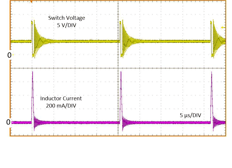
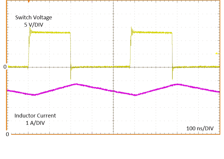
In PFM mode, the high-side MOSFET is turned on in a burst of one or more pulses to provide energy to the load. The duration of the burst depends on how long it takes the inductor current to reach IPEAK-MIN. The periodicity of these bursts is adjusted to regulate the output, while diode emulation (DEM) is used to maximize efficiency (see the Glossary). This mode provides high light-load efficiency by reducing the amount of input supply current required to regulate the output voltage at small loads. This trades off very good light-load efficiency for larger output voltage ripple and variable switching frequency. Also, a small increase in output voltage occurs at light loads. See Section 8.2.4 for output voltage variation with load in PFM mode. Figure 7-6 and Figure 7-7 show the typical switching waveforms in PFM and PWM.
There are four cases where the switching frequency does not conform to the condition set by the RT pin:
- Light load operation (AUTO mode)
- Dropout
- Minimum on-time operation
- Current limit
Under all of these cases, the switching frequency folds back, meaning it is less than that programmed by the RT control pin. During these conditions, by definition, the output voltage remains in regulation, except for current limit operation.
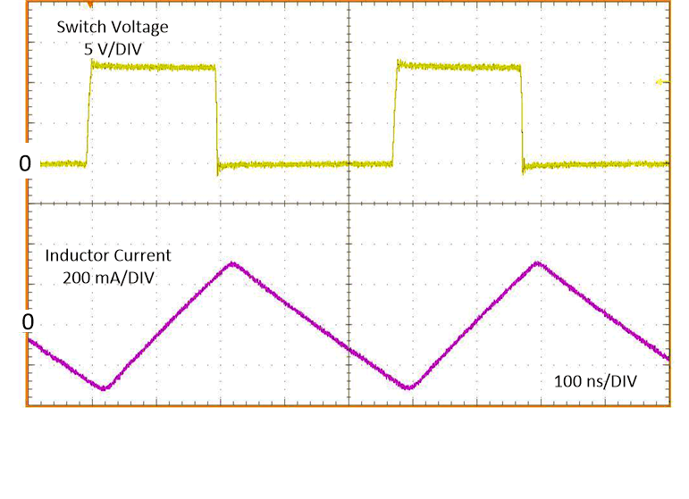
When the device is placed in forced PWM mode (FPWM), the switching frequency remains constant as programmed by the RT pin for all load conditions. This mode essentially turns off the light-load PFM frequency foldback mode detailed in Section 7.4.2. See Section 7.3.1 and Section 7.4.2.1 for details.
 Figure 7-6 Typical PFM Switching Waveforms VIN = 12 V, VOUT = 5
V, IOUT = 10 mA
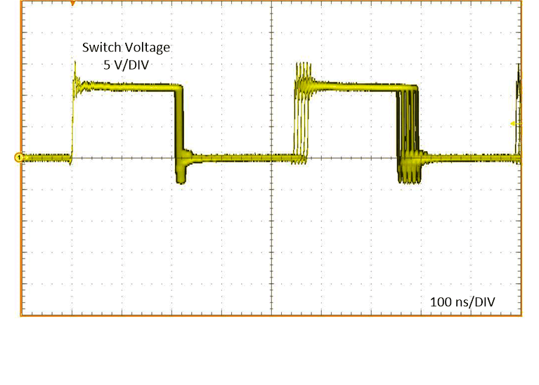
 Figure 7-8 Typical PWM Switching Waveforms With Spread Spectrum VIN = 12 V,
VOUT = 5 V, IOUT = 2.5 A, ƒSW = 2100
kHz
 Figure 7-7 Typical PWM Switching Waveforms Without Spread Spectrum VIN = 12
V, VOUT = 5 V, IOUT = 3.25 A, ƒSW = 2100
kHz
 Figure 7-9 Typical PWM Switching Waveforms FPWM VIN = 12 V, VOUT
= 5 V, IOUT = 0 A, ƒSW = 2100 kHz