JAJSSF1 January   2024 LM63635C-Q1

PRODUCTION DATA  

  1.   1
  2. 特長
  3. アプリケーション
  4. 概要
  5. Device Comparison Table
  6. Pin Configuration and Functions
  7. Specifications
    1. 6.1 Absolute Maximum Ratings
    2. 6.2 ESD Ratings
    3. 6.3 Recommended Operating Conditions
    4. 6.4 Thermal Information
    5. 6.5 Electrical Characteristics
    6. 6.6 Timing Characteristics
    7. 6.7 Switching Characteristics
    8. 6.8 System Characteristics
    9. 6.9 Typical Characteristics
  8. Detailed Description
    1. 7.1 Overview
    2. 7.2 Functional Block Diagram
    3. 7.3 Feature Description
      1. 7.3.1 Output Voltage Selection
      2. 7.3.2 Switching Frequency Selection
        1. 7.3.2.1 Spread Spectrum Option
      3. 7.3.3 Enable and Start-Up
      4. 7.3.4 RESET Flag Output
      5. 7.3.5 Undervoltage Lockout, Thermal Shutdown, and Output Discharge
    4. 7.4 Device Functional Modes
      1. 7.4.1 Overview
      2. 7.4.2 Light Load Operation
      3. 7.4.3 Dropout Operation
      4. 7.4.4 Minimum On-Time Operation
      5. 7.4.5 Current Limit and Short-Circuit Operation
  9. Application and Implementation
    1. 8.1 Application Information
    2. 8.2 Typical Application
      1. 8.2.1 Design Requirements
      2. 8.2.2 Detailed Design Procedure
        1. 8.2.2.1 Choosing the Switching Frequency
        2. 8.2.2.2 Inductor Selection
        3. 8.2.2.3 Output Capacitor Selection
        4. 8.2.2.4 Input Capacitor Selection
        5. 8.2.2.5 CBOOT
        6. 8.2.2.6 VCC
        7. 8.2.2.7 External UVLO
        8. 8.2.2.8 Maximum Ambient Temperature
      3. 8.2.3 Application Curves
      4. 8.2.4 EMI Performance Curves
    3. 8.3 Best Design Practices
    4. 8.4 Power Supply Recommendations
    5. 8.5 Layout
      1. 8.5.1 Layout Guidelines
        1. 8.5.1.1 Ground and Thermal Considerations
      2. 8.5.2 Layout Example
  10. Device and Documentation Support
    1. 9.1 Device Support
      1. 9.1.1 Device Nomenclature
    2. 9.2 Documentation Support
      1. 9.2.1 Related Documentation
    3. 9.3 ドキュメントの更新通知を受け取る方法
    4. 9.4 サポート・リソース
    5. 9.5 Trademarks
    6. 9.6 用語集
    7. 9.7 静電気放電に関する注意事項
  11. 10Revision History
  12. 11Mechanical, Packaging, and Orderable Information

パッケージ・オプション

メカニカル・データ(パッケージ|ピン)
サーマルパッド・メカニカル・データ
発注情報

Application Curves

Unless otherwise specified, the following conditions apply: VIN = 13.5V, TA = 25°C. Figure 8-1 shows the circuit with the appropriate BOM from Table 8-1.
GUID-CCBD343D-6E64-423B-99E5-F14F85047389-low.gif
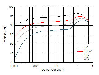
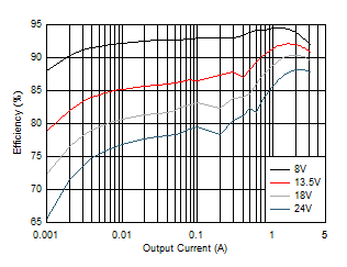
VOUT = 5V ƒSW = 2100kHz (auto)
Figure 8-5 Efficiency
GUID-0AD7C45A-702C-4E64-8020-DAC18A94651A-low.gif
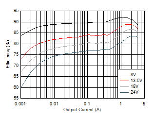
VOUT = 5V ƒSW = 400kHz (auto)
Figure 8-7 Efficiency
GUID-C31C3BAB-D812-4133-AEF4-42E487823308-low.gif
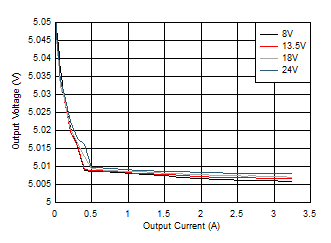
VOUT = 5V ƒSW = 2100kHz (auto)
Figure 8-9 Line and Load Regulation
GUID-E3B4E980-076D-4DFC-AF7B-4CA005B0FC7F-low.gif
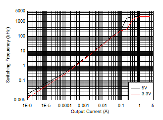
VIN = 13.5V ƒSW = 2100kHz (auto)
Figure 8-11 Switching Frequency versus Output Current
GUID-ED7E350E-FA96-44DB-8607-6B29436EFE4A-low.gif
VOUT = 5V
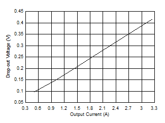
Figure 8-13 Dropout Voltage versus Output Current to 1.85MHz
GUID-BE460E86-1733-43D7-AD48-50EC6DE5F05C-low.gif
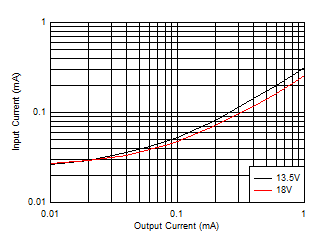
VOUT = 3.3V
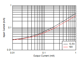
Figure 8-15 Input Supply Current versus Output Current
GUID-CC18870C-6E4D-4466-B6F7-BA2B82E38E88-low.gif
VOUT = 3.3V ƒSW = 2100kHz (auto)
Figure 8-6 Efficiency
GUID-44D22C69-C380-4126-8CF4-E8727D641DA0-low.gif
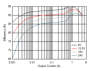
VOUT = 3.3V ƒSW = 400kHz (auto)
Figure 8-8 Efficiency
GUID-6641A523-ADA7-48EC-90E1-93D023B2D678-low.gif
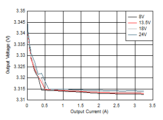
VOUT = 3.3V ƒSW = 2100kHz (auto)
Figure 8-10 Line and Load Regulation
GUID-690B6AD4-5B96-4557-B380-4D33D48561C6-low.gif
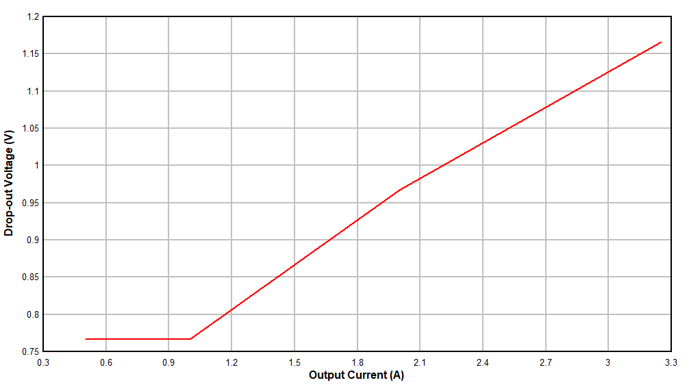
VOUT = 5V
Figure 8-12 Dropout Voltage versus Output Current for –1% Drop
GUID-95F8516F-F3A8-4023-8C54-60A760DF7D94-low.gif
VOUT = 5V
Figure 8-14 Input Supply Current versus Output Current