JAJSJO5B October 2022 – August 2024 LM64440-Q1 , LM64460-Q1
PRODUCTION DATA
- 1
- 1 特長
- 2 アプリケーション
- 3 概要
- 4 Device Comparison Table
- 5 Pin Configuration and Functions
- 6 Specifications
-
7 Detailed Description
- 7.1 Overview
- 7.2 Functional Block Diagram
- 7.3
Feature Description
- 7.3.1 Input Voltage Range (VIN1, VIN2)
- 7.3.2 Output Voltage Setpoint (FB)
- 7.3.3 Precision Enable and Input Voltage UVLO (EN)
- 7.3.4 MODE/SYNC Operation
- 7.3.5 Clock Locking
- 7.3.6 Power-Good Monitor (PGOOD)
- 7.3.7 Bias Supply Regulator (VCC, BIAS)
- 7.3.8 Bootstrap Voltage and UVLO (CBOOT)
- 7.3.9 Spread Spectrum
- 7.3.10 Soft Start and Recovery From Dropout
- 7.3.11 Overcurrent and Short-Circuit Protection
- 7.3.12 Thermal Shutdown
- 7.3.13 Input Supply Current
- 7.4 Device Functional Modes
-
8 Application and Implementation
- 8.1 Application Information
- 8.2
Typical Applications
- 8.2.1 Design 1 – Automotive Synchronous 6A Buck Regulator at 2.1MHz
- 8.2.2
Design 2 – Automotive Synchronous 4A Buck Regulator at 2.1MHz
- 8.2.2.1 Design Requirements
- 8.2.2.2
Detailed Design Procedure
- 8.2.2.2.1 Custom Design With WEBENCH® Tools
- 8.2.2.2.2 Setting the Output Voltage
- 8.2.2.2.3 Choosing the Switching Frequency
- 8.2.2.2.4 Inductor Selection
- 8.2.2.2.5 Output Capacitor Selection
- 8.2.2.2.6 Input Capacitor Selection
- 8.2.2.2.7 Bootstrap Capacitor
- 8.2.2.2.8 VCC Capacitor
- 8.2.2.2.9 BIAS Power Connection
- 8.2.2.2.10 Feedforward Network
- 8.2.2.2.11 Input Voltage UVLO
- 8.2.2.3 Application Curves
- 8.3 Power Supply Recommendations
- 8.4 Layout
- 9 Device and Documentation Support
- 10Revision History
- 11Mechanical, Packaging, and Orderable Information
7.4.3.2.2 Frequency Foldback
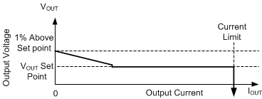
The converter reduces the switching frequency whenever the output voltage is higher than the setpoint. This function is enabled whenever COMP, an internal signal, is low and there is an offset between the FB regulation setpoint and the voltage applied at FB. The net effect is that there is a larger output impedance while lightly loaded in AUTO mode than in normal operation. The output voltage is approximately 1% high when the converter is completely unloaded.

In PFM operation, a small DC positive offset is required on the output voltage to activate the PFM detector. The lower the frequency in PFM, the more DC offset is needed on VOUT. If the DC offset on VOUT is not acceptable, use a dummy load at the output or select FPWM mode to reduce or eliminate this offset.