JAJSM18A November   2021  – March 2022 LM66100-Q1

PRODUCTION DATA  

  1. 特長
  2. アプリケーション
  3. 概要
  4. Revision History
  5. Pin Configuration and Functions
  6. Specifications
    1. 6.1 Absolute Maximum Ratings
    2. 6.2 ESD Ratings
    3. 6.3 Recommended Operating Conditions
    4. 6.4 Thermal Information
    5. 6.5 Electrical Characteristics
    6. 6.6 Switching Characteristics
    7. 6.7 Typical Characteristics
  7. Parameter Measurement Information
  8. Detailed Description
    1. 8.1 Overview
    2. 8.2 Functional Block Diagram
    3. 8.3 Feature Description
      1. 8.3.1 Reverse Polarity Protection (RPP)
      2. 8.3.2 Always-ON Reverse Current Blocking (RCB)
    4. 8.4 Device Functional Modes
  9. Application and Implementation
    1. 9.1 Application Information
    2. 9.2 Typical Applications
      1. 9.2.1 Dual Ideal Diode ORing
        1. 9.2.1.1 Design Requirements
        2. 9.2.1.2 Detailed Design Procedure
        3. 9.2.1.3 Application Curves
      2. 9.2.2 Dual Ideal Diode ORing for Continuous Output Power
        1. 9.2.2.1 Design Requirements
        2. 9.2.2.2 Application Curves
      3. 9.2.3 ORing with Discrete MOSFET
        1. 9.2.3.1 Design Requirements
        2. 9.2.3.2 Application Curves
  10. 10Power Supply Recommendations
  11. 11Layout
    1. 11.1 Layout Guidelines
    2. 11.2 Layout Example
  12. 12Device and Documentation Support
    1. 12.1 Receiving Notification of Documentation Updates
    2. 12.2 サポート・リソース
    3. 12.3 Trademarks
    4. 12.4 Electrostatic Discharge Caution
    5. 12.5 Glossary
  13. 13Mechanical, Packaging, and Orderable Information

パッケージ・オプション

メカニカル・データ(パッケージ|ピン)
サーマルパッド・メカニカル・データ
発注情報

Application Curves

The below scope shot shows the output voltage (VOUT) being initially powered by VIN1. When VIN2 is applied, it powers VOUT because it is a higher voltage. When VIN2 is removed, VOUT is once again powered by VIN1.
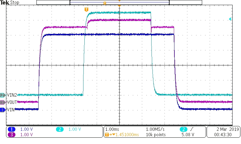
GUID-D2F0FD4F-2BB8-4BA4-8B06-A55C46BA19C8-low.jpg
Figure 9-2 Dual Ideal Diode ORing Behavior