JAJSKQ1 November   2021 LM66200

PRODUCTION DATA  

  1. 特長
  2. アプリケーション
  3. 概要
  4. Revision History
  5. Pin Configuration and Functions
  6. Specifications
    1. 6.1 Absolute Maximum Ratings
    2. 6.2 ESD Ratings
    3. 6.3 Recommended Operating Conditions
    4. 6.4 Thermal Information
    5. 6.5 Electrical Characteristics
    6. 6.6 Switching Characteristics
    7. 6.7 Typical Characteristics
  7. Detailed Description
    1. 7.1 Overview
    2. 7.2 Functional Block Diagram
    3. 7.3 Feature Description
      1. 7.3.1 Truth Table
      2. 7.3.2 Soft Start
      3. 7.3.3 Status Indication
    4. 7.4 VINx Collapse Rate
    5. 7.5 Output Voltage Drop
    6. 7.6 Device Functional Modes
      1. 7.6.1 Automatic Switchover
  8. Application and Implementation
    1. 8.1 Application Information
    2. 8.2 Typical Application
      1. 8.2.1 Design Requirements
      2. 8.2.2 Detailed Design Procedure
      3. 8.2.3 Application Performance Plots
  9. Power Supply Recommendations
  10. 10Layout
    1. 10.1 Layout Guidelines
    2. 10.2 Layout Example
  11. 11Device and Documentation Support
    1. 11.1 Documentation Support
      1. 11.1.1 Related Documentation
    2. 11.2 Receiving Notification of Documentation Updates
    3. 11.3 Trademarks
    4. 11.4 Electrostatic Discharge Caution
    5. 11.5 Glossary
  12. 12Mechanical, Packaging, and Orderable Information

パッケージ・オプション

メカニカル・データ(パッケージ|ピン)
サーマルパッド・メカニカル・データ
発注情報

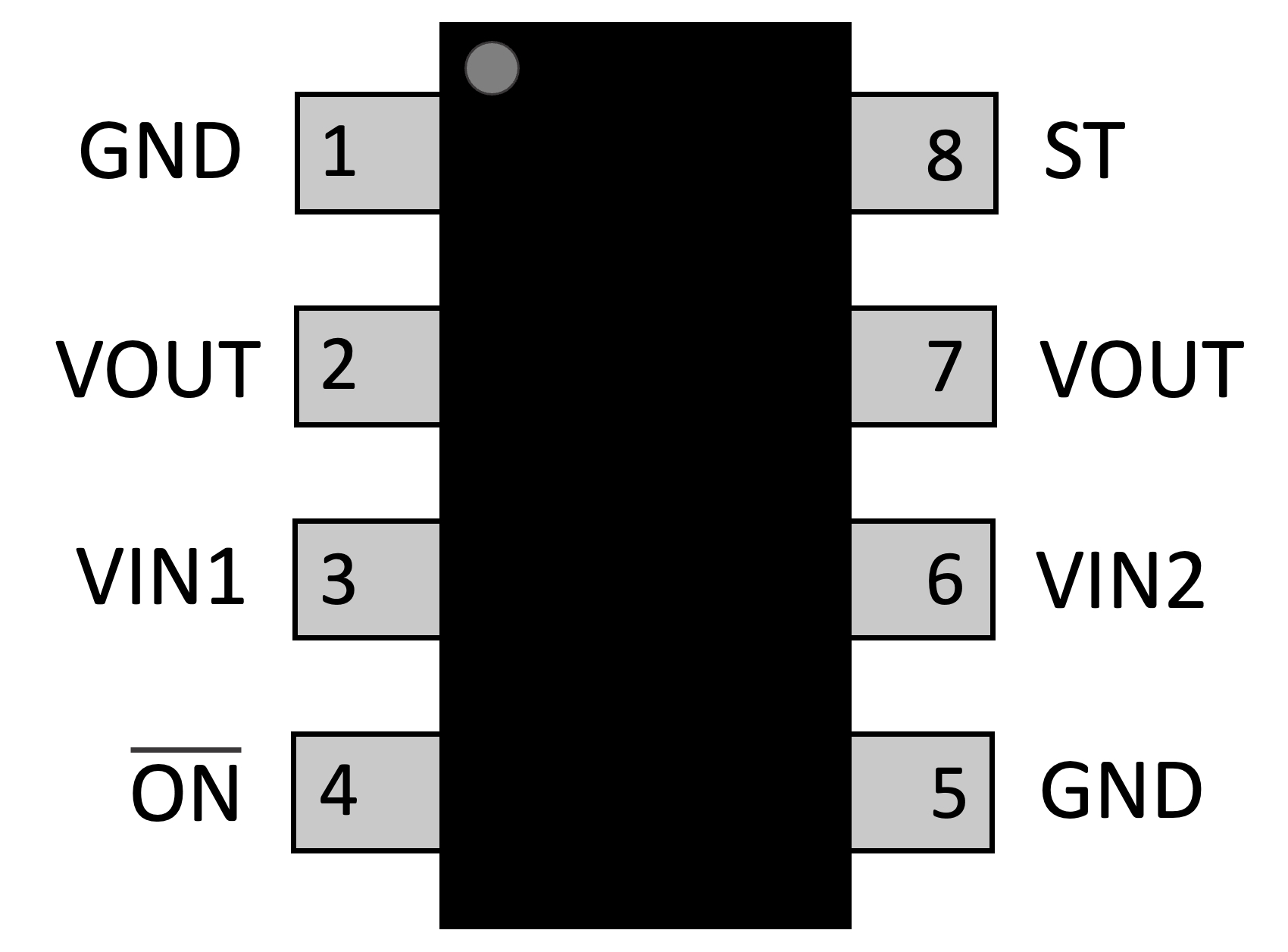
Pin Configuration and Functions

GUID-20211029-SS0I-ZSWX-BW6L-HKVM7CPFCNXZ-low.jpgFigure 5-1 DRL Package8-Pin SOTTop View
Table 5-1 Pin Functions
PINI/ODESCRIPTION
NAMENO.
GND1, 5Device ground
VOUT2, 7OOutput power
VIN13IChannel 1 input power

ON

4I

Active low enable pin. Device is enabled when ON is pulled low and the device turns off both channels when ON is pulled high.

VIN26IChannel 2 input power
ST8OStatus pin. Pulled high when VIN1 is being used and pulled low when VIN2 is being used. Can be pulled up to VIN1 to reduce quiescent current when VIN2 is powering the output.