JAJSCV4 December 2016 LM73-Q1
PRODUCTION DATA.
- 1 特長
- 2 アプリケーション
- 3 概要
- 4 改訂履歴
- 5 Pin Configuration and Functions
- 6 Specifications
- 7 Detailed Description
- 8 Application and Implementation
- 9 Power Supply Recommendations
- 10Layout
- 11デバイスおよびドキュメントのサポート
- 12メカニカル、パッケージ、および注文情報
8 Application and Implementation
NOTE
Information in the following applications sections is not part of the TI component specification, and TI does not warrant its accuracy or completeness. TI’s customers are responsible for determining suitability of components for their purposes. Customers should validate and test their design implementation to confirm system functionality.
8.1 Application Information
8.1.1 Thermal Path Considerations
To get the expected results when measuring temperature with an integrated circuit temperature sensor like the LM73-Q1, it is important to understand that the sensor measures its own die temperature. For the LM73-Q1, the best thermal path between the die and the outside world is through the LM73-Q1's pins. In the SOT23 package, all the pins on the LM73-Q1 will have an equal effect on the die temperature. Because the pins represent a good thermal path to the LM73-Q1 die, the LM73-Q1 will provide an accurate measurement of the temperature of the printed circuit board on which it is mounted. There is a less efficient thermal path between the plastic package and the LM73-Q1 die. If the ambient air temperature is significantly different from the printed circuit board temperature, it will have a small effect on the measured temperature.
8.1.2 Output Considerations: Tight Accuracy, Resolution and Low Noise
The LM73-Q1 is well suited for applications that require tight temperature measurement accuracy. In many applications, the low temperature error can mean better system performance and, by eliminating a system calibration step, lower production cost.
With digital resolution as fine as 0.03125 °C/LSB, the LM73-Q1 senses and reports very small changes in its temperature, making it ideal for applications where temperature sensitivity is important. For example, the LM73-Q1 enables the system to quickly identify the direction of temperature change, allowing the processor to take compensating action before the system reaches a critical temperature.
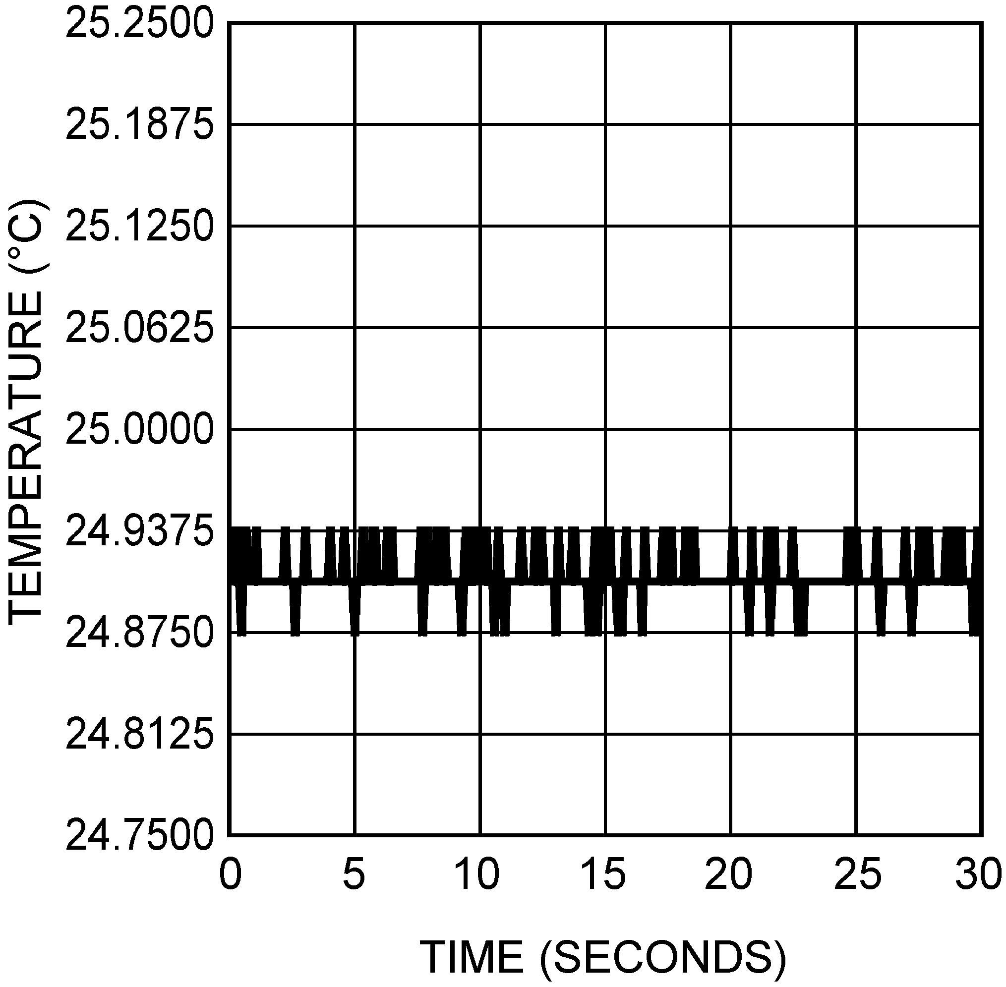
The LM73-Q1 has very low output noise, typically 0.015°C rms, which makes it ideal for applications where stable thermal compensation is a priority. For example, in a temperature-compensated oscillator application, the very small deviation in successive temperature readings translates to a stable frequency output from the oscillator.
8.2 Typical Application
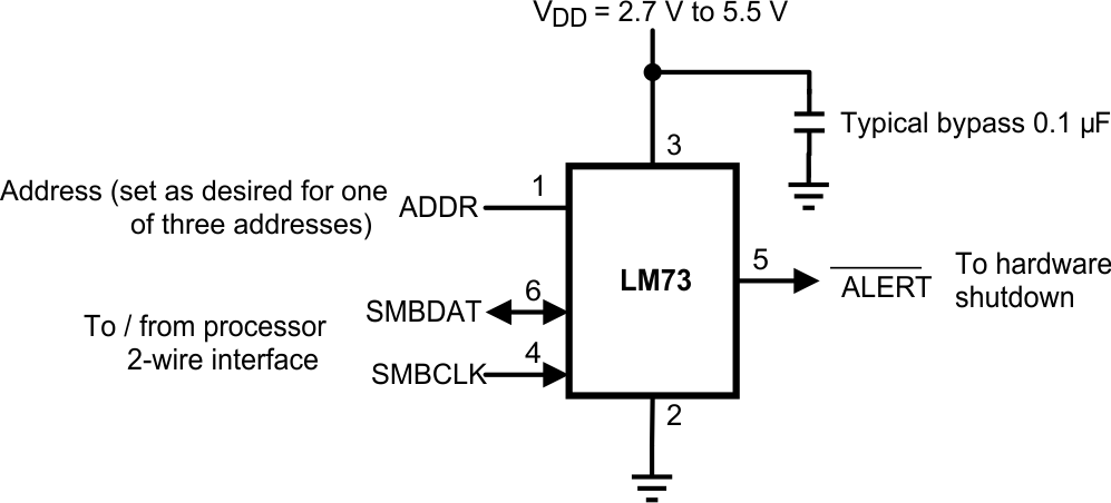
 Figure 13. Digital Temperature Sensing
8.2.1 Design Requirements
The LM73-Q1 requires positive supply voltage of 2.7 V to 5.5 V to be applied between +VDD and GND. For best results, bypass capacitors of 100 nF and 10 μF are recommended.
8.2.2 Detailed Design Procedure
The temperature resolution is programmable, allowing the host system to select the optimal configuration between sensitivity and conversion time. The LM73-Q1 can be placed in shutdown to minimize power consumption when temperature data is not required. While in shutdown, a 1-shot conversion mode allows system control of the conversion rate for ultimate flexibility.
8.2.3 Application Curve
 Figure 14. Typical Performance