JAJS911I August 1999 – May 2016 LM7301
PRODUCTION DATA.
- 1 特長
- 2 アプリケーション
- 3 概要
- 4 改訂履歴
- 5 Pin Configuration and Functions
- 6 Specifications
- 7 Detailed Description
- 8 Applications and Implementation
- 9 Power Supply Recommendations
- 10Layout
- 11デバイスおよびドキュメントのサポート
- 12メカニカル、パッケージ、および注文情報
パッケージ・オプション
メカニカル・データ(パッケージ|ピン)
サーマルパッド・メカニカル・データ
発注情報
8 Applications and Implementation
NOTE
Information in the following applications sections is not part of the TI component specification, and TI does not warrant its accuracy or completeness. TI’s customers are responsible for determining suitability of components for their purposes. Customers should validate and test their design implementation to confirm system functionality.
8.1 Application Information
8.1.1 Handheld Remote Controls
The LM7301 offers outstanding specifications for applications requiring good speed/power trade-off. In applications such as remote control operation, where high bandwidth and low power consumption are needed, the LM7301 performance can easily meet these requirements.
8.1.2 Remote Microphone in Personal Computers
Remote microphones in Personal Computers often use a microphone at the top of the monitor which must drive a long cable in a high noise environment. One method often used to reduce the nose is to lower the signal impedance, which reduces the noise pickup. In this configuration, the amplifier usually requires 30 db to 40 db of gain, at bandwidths higher than most low-power CMOS parts can achieve. The LM7301 offers the tiny package, higher bandwidths, and greater output drive capability than other rail-to-rail input/output parts can provide for this application.
8.1.3 Optical Line Isolation for Modems
The combination of the low distortion and good load driving capabilities of the LM7301 make it an excellent choice for driving opto-coupler circuits to achieve line isolation for modems. This technique prevents telephone line noise from coupling onto the modem signal. Superior isolation is achieved by coupling the signal optically from the computer modem to the telephone lines; however, this also requires a low distortion at relatively high currents. Due to its low distortion at high-output drive currents, the LM7301 fulfills this need, in this and in other telecom applications. See Stability Considerations for methods used to ensure stability under all load conditions.
8.2 Typical Applications
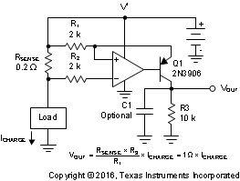
The circuit shown in Figure 27 uses the wide supply voltage range (1.8 V to 32 V), rail-to-rail input and output voltage capability, and the unity gain stability of the LM7301 to sense the current flow from the power supply to a load, such as a battery being charged, or any other load. The circuit creates a ground-referenced output voltage, which varies linearly with the load current, for easy interface to the rest of the circuitry to create fault-protection, current and power metering, or current regulation functions.
 Figure 27. High Side Current Sensing
8.2.1 Design Requirements
The output port is designed for easy interface; it is ground-referenced and it produces 0 V with 0 A of load current. A typical stage that follows this stage, an ADC which samples the load current for example, is easily connected to the Q1 collector with no level shifting or additional biasing required.
Apart from a wide supply voltage capability, the operational amplifier used in Figure 27 must have an input voltage range that includes the V+ rail voltage to allow high side current sensing. Furthermore, it should be unity gain stable and have an output voltage range which is less than one Vbe from V+. The LM7301 has all these requirements.
8.2.2 Detailed Design Procedure
8.2.2.1 Selecting RSENSE
Pick the value of RSENSE low enough to minimize its heat / voltage loss while observing Equation 1 for minimum detectable load current, ICHARGE_MIN , and device offset voltage, VOS:

With the schematic values shown and LM7301's VOS limit of 6 mV:

If the system has the ability to be initialized and corrected for initial readings, it may be possible to lower the value of RSENSE.
8.2.2.2 Selecting R1, and R3 Values
Pick the R3 / R1 ratio to get the proper full-scale VOUT when the maximum load current, ICHARGE_MAX, flows:

For example, to get 3-V output with 3 A of load current when RSENSE = 0.2 Ω results in:

Ensure that the resulting transfer function also satisfies the application’s need when the minimum load current, ICHARGE_MIN is being sensed. In this example, the minimum output voltage will be 30 mV (when ICHARGE_MIN = 30 mA).
With the R3/R1 ratio determined, pick the value of R3 for Q1 collector current less than 1 mA at the maximum VOUT, and determine R1 from that.
8.2.2.3 R1, R2 Selection
Normally, R2 is set equal to R1 to cancel out the error term due to the input bias current, IB (approximately 200 nA for the LM7301).
8.2.2.4 Error Terms Expressions
Here are the expressions for the output change caused by various parameter shifts, evaluated for Figure 27 values with ICHARGE_MAX= 3 A:
Offset Voltage, ΔVOS:

Offset current, IOS:

Self-heating of RSENSE causing ΔRSENSE with ICHARGE_MAX flowing:

8.2.2.5 Frequency Response
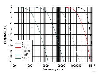
Depending on the application, it may be useful to have the means to control the upper end of the circuit’s frequency response. An example is limiting the circuit’s response to high-frequency load current spikes or switching frequencies so that the circuit only reacts to DC or lower frequencies. Capacitor C1 in Figure 27 can be used to accomplish just that. The original circuit has a –3-dB bandwidth close to 4.5 MHz which can be reduced by increasing the value of C1, as shown in Figure 28.
 Figure 28. Current Sense Frequency Response vs C1 Value
8.2.3 Application Curves
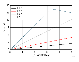
Figure 29 shows the transfer function of the circuit for several values of RSENSE. Notice that with 1 Ω, the output is limited to approximately 16 V because of the additional drop across the sense resistor at higher load currents.
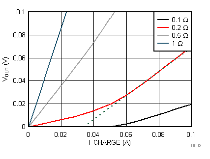
Figure 30 shows the low-end of the load current is more non-linear for low RSENSE values, as noted in Selecting RSENSE due to VOS. Higher RSENSE values help with this at the expense of a higher loss and voltage drop.

| Use lower sense resistor value to avoid voltage limitation! |

| Line showing linearity degradation at the lower end. |