JAJSMA4A July 2021 – February 2022 LM74501-Q1
PRODUCTION DATA
- 1 特長
- 2 アプリケーション
- 3 概要
- 4 Revision History
- 5 Pin Configuration and Functions
- 6 Specifications
- 7 Parameter Measurement Information
- 8 Detailed Description
- 9 Application and Implementation
- 10Power Supply Recommendations
- 11Layout
- 12Device and Documentation Support
- 13Mechanical, Packaging, and Orderable Information
パッケージ・オプション
デバイスごとのパッケージ図は、PDF版データシートをご参照ください。
メカニカル・データ(パッケージ|ピン)
- DDF|8
サーマルパッド・メカニカル・データ
発注情報
8.3.6 Gate Discharge Timer
The LM74501-Q1 has a unique gate discharge timer feature, which enables TVS less reverse polarity protection solution in case of ISO7637-2 pulse 1 event. An additional capacitor (CT) across external N-FET's GATE to SOURCE terminal keeps external N-FET on for specific time window even when input voltage falls below VPORF threshold of SOURCE pin or when the EN pin is pulled low. This gate discharge feature allows reverse current back to input source by keeping external MOSFET on for extended time duration set by gate discharge timer capacitor (CT) and enables automotive systems to meet TVS less ISO 7637-2 pulse 1 operation. Use Equation 2 to calculate the typical gate discharge time.
Where
- RD is the LM74501-Q1 internal GATE discharge resistor (typically 30 kΩ).
- Ciss is the external MOSFET input capacitance.
- CT is the timer capacitor connected between GATE and SOURCE of an external MOSFET.
- VT is the gate-to-source threshold voltage of an external MOSFET.
- VGATE is the nominal GATE pin voltage of LM74501-Q1 (12.4-V typical).
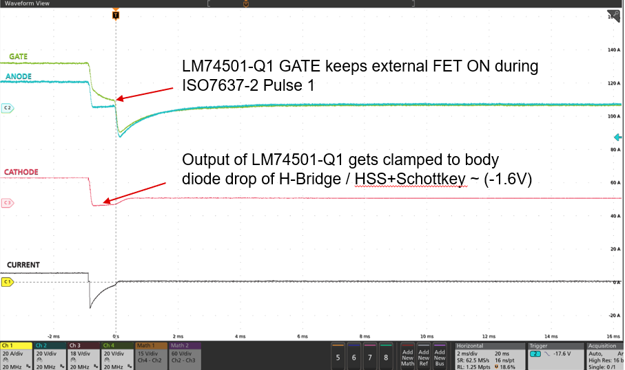
Figure 8-3 shows equivalent the LM74501-Q1 circuit operation during an ISO7637-2 pulse 1 event. Note that reverse current flows back to the input source from output loads such as a high-side switch followed by schottky diode or MOSFET H-bridge driving motor load. Thus, to achieve TVS less operation during ISO7637-2 pulse 1 events, output loads must be capable of withstanding the peak reverse current during ISO7637-2 pulse 1 event.
Figure 8-4 shows the TVS-less ISO7637-2 pulse 1 performance of the LM74501-Q1 with output loads capable of handling reverse current during an ISO7637-2 pulse 1 event, similar to loads configuration shown in Figure 8-4.
 Figure 8-4 TVS Less Operation During ISO7637-2 Pulse 1
The other short duration transient events such as ISO7637-2 pulse 2A, 3A, or 3B usually get filtered out by input and output capacitors and do not affect the system performance.
For the loads that cannot handle peak reverse current during an ISO 7637-2 pulse 1 transient event but can handle negative voltage for a short duration, a schottky diode capable of handling peak reverse current can be placed from output to ground to clamp the output voltage to negative forward voltage drop of the Schottky diode (–VF).