JAJSM17A December   2021  – May 2022 LM74502 , LM74502H

PRODUCTION DATA  

  1. 特長
  2. アプリケーション
  3. 概要
  4. Revision History
  5. Pin Configuration and Functions
  6. Specifications
    1. 6.1 Absolute Maximum Ratings
    2. 6.2 ESD Ratings
    3. 6.3 Recommended Operating Conditions
    4. 6.4 Thermal Information
    5. 6.5 Electrical Characteristics
    6. 6.6 Switching Characteristics
    7. 6.7 Typical Characteristics
  7. Parameter Measurement Information
  8. Detailed Description
    1. 8.1 Overview
    2. 8.2 Functional Block Diagram
    3. 8.3 Feature Description
      1. 8.3.1 Input Voltage
      2. 8.3.2 Charge Pump (VCAP)
      3. 8.3.3 Gate Driver (GATE, SRC)
        1. 8.3.3.1 Inrush Current Control
      4. 8.3.4 Enable (EN/UVLO)
      5. 8.3.5 Overvoltage Protection (OV)
    4. 8.4 Device Functional Modes
      1. 8.4.1 Shutdown Mode
      2. 8.4.2 Conduction Mode
  9. Application and Implementation
    1. 9.1 Application Information
    2. 9.2 Typical Application
      1. 9.2.1 Design Requirements
      2. 9.2.2 Detailed Design Procedure
        1. 9.2.2.1 Design Considerations
        2. 9.2.2.2 MOSFET Selection
        3. 9.2.2.3 Overvoltage Protection
        4. 9.2.2.4 Charge Pump VCAP, Input and Output Capacitance
      3. 9.2.3 Application Curves
    3. 9.3 Input Surge Stopper Using LM74502, LM74502H
      1. 9.3.1 VS Capacitance, Resistor R1 and Zener Clamp (DZ)
      2. 9.3.2 Overvoltage Protection
      3. 9.3.3 MOSFET Selection
    4. 9.4 Fast Turn-On and Turn-Off High Side Switch Driver Using LM74502H
  10. 10Power Supply Recommendations
  11. 11Layout
    1. 11.1 Layout Guidelines
    2. 11.2 Layout Example
  12. 12Device and Documentation Support
    1. 12.1 Receiving Notification of Documentation Updates
    2. 12.2 サポート・リソース
    3. 12.3 Trademarks
    4. 12.4 Electrostatic Discharge Caution
    5. 12.5 Glossary
  13. 13Mechanical, Packaging, and Orderable Information

パッケージ・オプション

メカニカル・データ(パッケージ|ピン)
サーマルパッド・メカニカル・データ
発注情報

MOSFET Selection

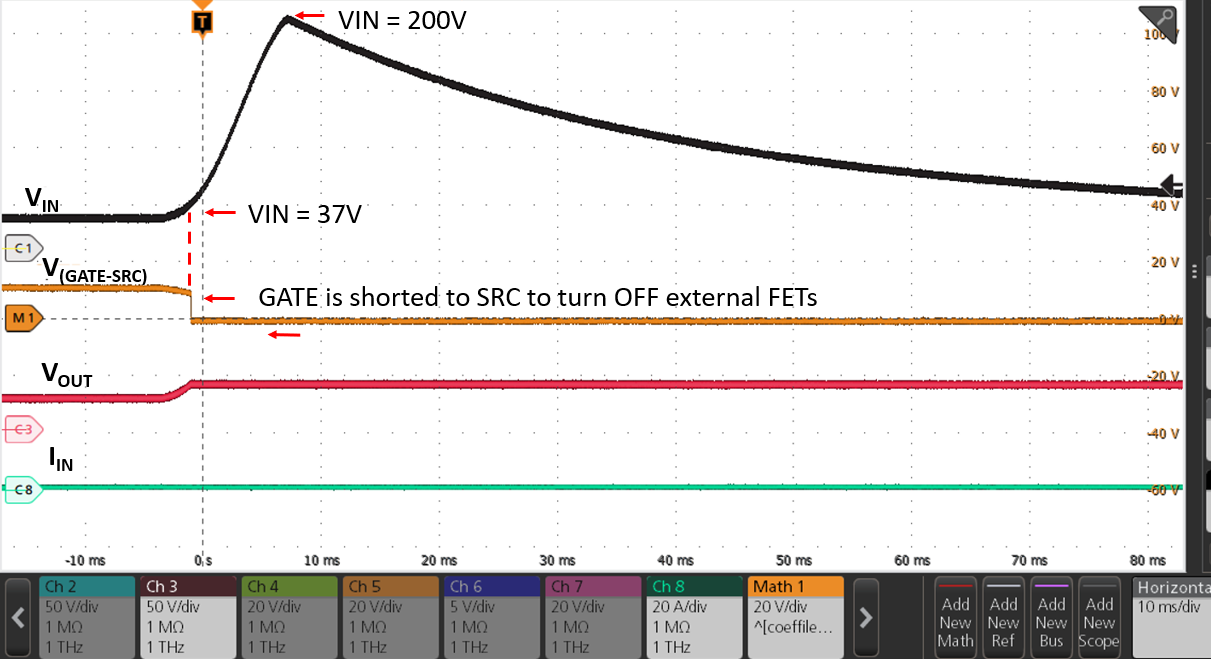
The VDS rating of the MOSFET Q1 must be minimum VIN(max) for designs with output overvoltage cutoff where output can reach 0 V with higher loads. For designs with output overvoltage clamp, MOSFET VDS rating must be (VIN(max) – VOUT_CLAMP). The VGS rating is based on GATE-SRC maximum voltage of 15 V. TI recommends a 20-V VGS rated MOSFET. Power dissipation on MOSFET Q1 on a design where output is clamped is critical and SOA characteristics of the MOSFET must be considered with sufficient design margin for reliable operation. An additional zener diode from GATE to SRC can be needed to protect the external FET in case output is expected to drop to the level where it can exceed external FET VGS(max) rating.
GUID-20211208-SS0I-DSK4-M6LN-6MQFVNWZT6W8-low.pngFigure 9-9 200-V Surge Stopper with Overvoltage Cutoff Using LM74502