JAJSM66A June   2021  – December 2021 LM74701-Q1

PRODUCTION DATA  

  1. 特長
  2. アプリケーション
  3. 概要
  4. Revision History
  5. Pin Configuration and Functions
  6. Specifications
    1. 6.1 Absolute Maximum Ratings
    2. 6.2 ESD Ratings
    3. 6.3 Recommended Operating Conditions
    4. 6.4 Thermal Information
    5. 6.5 Electrical Characteristics
    6. 6.6 Switching Characteristics
    7. 6.7 Typical Characteristics
  7. Parameter Measurement Information
  8. Detailed Description
    1. 8.1 Overview
    2. 8.2 Functional Block Diagram
    3. 8.3 Feature Description
      1. 8.3.1 Input Voltage
      2. 8.3.2 Charge Pump
      3. 8.3.3 Gate Driver
      4. 8.3.4 Enable
      5. 8.3.5 Battery Voltage Monitoring (SW)
    4. 8.4 Device Functional Modes
      1. 8.4.1 Shutdown Mode
      2. 8.4.2 Conduction Mode
        1. 8.4.2.1 Regulated Conduction Mode
        2. 8.4.2.2 Full Conduction Mode
        3. 8.4.2.3 VDS Clamp Mode
      3. 8.4.3 Reverse Current Protection Mode
  9. Application and Implementation
    1. 9.1 Application Information
    2. 9.2 Typical Application
      1. 9.2.1 Design Requirements
      2. 9.2.2 Detailed Design Procedure
        1. 9.2.2.1 Design Considerations
        2. 9.2.2.2 MOSFET Selection
        3. 9.2.2.3 Charge Pump VCAP (CVCAP) and Input Capacitance (CIN)
        4. 9.2.2.4 Output Capacitance (COUT)
      3. 9.2.3 Application Curves
    3. 9.3 What to Do and What Not to Do
    4. 9.4 OR-ing Application Configuration
  10. 10Power Supply Recommendations
  11. 11Layout
    1. 11.1 Layout Guidelines
    2. 11.2 Layout Example
  12. 12Device and Documentation Support
    1. 12.1 Receiving Notification of Documentation Updates
    2. 12.2 サポート・リソース
    3. 12.3 Trademarks
    4. 12.4 Electrostatic Discharge Caution
    5. 12.5 Glossary
  13. 13Mechanical, Packaging, and Orderable Information

パッケージ・オプション

デバイスごとのパッケージ図は、PDF版データシートをご参照ください。

メカニカル・データ(パッケージ|ピン)
  • DDF|8
サーマルパッド・メカニカル・データ
発注情報

Typical Characteristics

Figure 6-1 Shutdown Supply Current vs Supply Voltage
Figure 6-3 Anode Current vs Negative Supply Voltage
Figure 6-5 Charge Pump Current vs Supply Voltage at VCAP = 6 V
Figure 6-7 Charge Pump V-I Characteristics at VANODE = 3.2 V
Figure 6-9 Reverse Current Blocking Delay vs Temperature
Figure 6-11 Enable to Gate Delay vs Temperature
Figure 6-13 Charge Pump UVLO Threshold vs Temperature
Figure 6-15 VDSCLAMP Threshold vs Temperature
Figure 6-2 Operating Quiescent Current vs Supply Voltage
Figure 6-4 CATHODE Sink Current vs Supply Voltage
Figure 6-6 Charge Pump V-I Characteristics at VANODE > = 12 V
Figure 6-8 Enable Falling threshold vs Temperature
Figure 6-10 Forward Recovery Delay vs Temperature
Figure 6-12 Charge Pump ON and OFF Threshold vs Temperature
Figure 6-14 VANODE POR Threshold vs Temperature
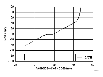
GUID-282095A9-DA1E-4BDF-A71F-70B8E795213D-low.gifFigure 6-16 Gate Current vs Forward Voltage Drop