JAJSM66A June 2021 – December 2021 LM74701-Q1
PRODUCTION DATA
- 1 特長
- 2 アプリケーション
- 3 概要
- 4 Revision History
- 5 Pin Configuration and Functions
- 6 Specifications
- 7 Parameter Measurement Information
- 8 Detailed Description
- 9 Application and Implementation
- 10Power Supply Recommendations
- 11Layout
- 12Device and Documentation Support
- 13Mechanical, Packaging, and Orderable Information
パッケージ・オプション
デバイスごとのパッケージ図は、PDF版データシートをご参照ください。
メカニカル・データ(パッケージ|ピン)
- DDF|8
サーマルパッド・メカニカル・データ
発注情報
5 Pin Configuration and Functions
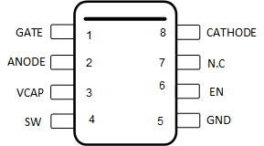
 Figure 5-1 DDF Package 8-Pin SOT-23 Top View
Table 5-1 Pin Functions
| PIN | I/O(1) | DESCRIPTION | |
|---|---|---|---|
| NO. | NAME | ||
| 1 | GATE | O | Gate drive output. Connect to gate of the external N-channel MOSFET. |
| 2 | ANODE | I | Anode of the ideal diode and input power. Connect to the source of the external N-channel MOSFET. |
| 3 | VCAP | O | Charge pump output. Connect to external charge pump capacitor. |
| 4 | SW | O | Voltage sensing disconnect switch terminal. ANODE and SW are internally connected through a switch when EN is high. A resistor ladder from this pin to GND can be used to monitor battery voltage. When EN is pulled low, the switch is OFF disconnecting the resistor ladder from the battery line thereby cutting off the leakage current. |
| 5 | GND | G | Ground pin |
| 6 | EN | I | Enable pin. Can be connected to ANODE for always ON operation. |
| 7 | N.C | — | No connect. Keep this pin floating. |
| 8 | CATHODE | I | Cathode of the ideal diode. Connect to the drain of the external N-channel MOSFET. |
(1) I = Input, O = Output, G = GND