JAJSFG5D November 2008 – May 2018 LM7705
PRODUCTION DATA.
- 1 特長
- 2 アプリケーション
- 3 概要
- 4 改訂履歴
- 5 Pin Configuration and Functions
- 6 Specifications
- 7 Detailed Description
- 8 Application and Implementation
- 9 Power Supply Recommendations
- 10Layout
- 11デバイスおよびドキュメントのサポート
- 12メカニカル、パッケージ、および注文情報
6.7 Typical Characteristics
VDD = 3.3 V and TA = 25°C unless otherwise noted.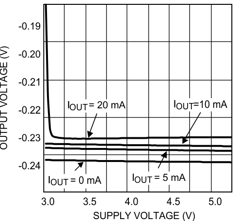 Figure 1. Output Voltage vs. Supply Voltage
 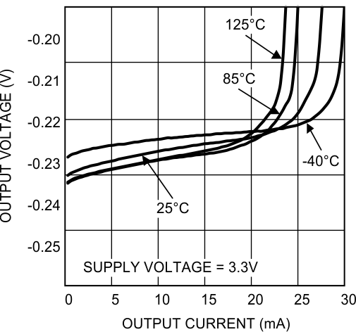 Figure 3. Output Voltage vs. Output Current
  Figure 5. Output Voltage Ripple vs. Temperature
 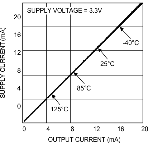 Figure 7. Supply Current vs. Output Current
  Figure 9. Current Conversion Efficiency vs. Output Current
  Figure 11. Turnon Time
  Figure 13. Load Regulation vs. Temperature
  Figure 15. Transient Response
  Figure 17. Transient Response
  Figure 19. Output voltage vs. Shutdown Voltage
  Figure 21. Oscillator Frequency vs. Temperature
  Figure 2. Supply Current vs. Supply Voltage
  Figure 4. Output Voltage vs. Output Current
  Figure 6. Output Voltage Ripple vs. Temperature
  Figure 8. Supply Current vs. Output Current
 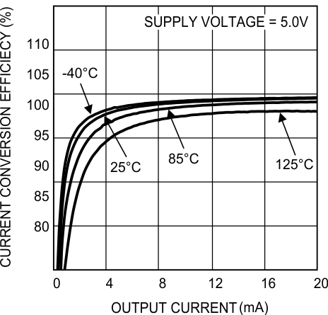 Figure 10. Current Conversion Efficiency vs. Output Current
  Figure 12. Turnon Time
  Figure 14. Load Regulation vs. Temperature
 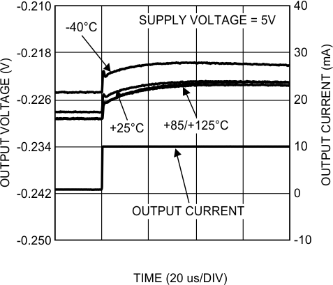 Figure 16. Transient Response
 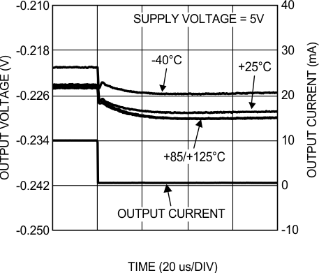 Figure 18. Transient Response
  Figure 20. Supply Current vs. Shutdown Voltage