JAJSDG6
June 2017
LM78M05-MIL
PRODUCTION DATA.
1
特長
2
アプリケーション
3
概要
4
改訂履歴
5
Pin Configuration and Functions
6
Specifications
6.1
Absolute Maximum Ratings
6.2
Recommended Operating Conditions
6.3
Thermal Information
6.4
Electrical Characteristics
6.5
Typical Characteristics
7
Detailed Description
7.1
Overview
7.2
Functional Block Diagram
7.3
Feature Description
7.4
Device Functional Modes
7.4.1
Normal Operation
7.4.2
Operation With Low Input Voltage
7.4.3
Operation in Self Protection
8
Application and Implementation
8.1
Application Information
8.2
Typical Application
8.2.1
Design Requirements
8.2.2
Detailed Design Procedure
8.2.2.1
Input Voltage
8.2.2.2
Output Current
8.2.2.3
Input Capacitor
8.2.2.4
Output Capacitor
8.2.3
Application Curves
9
Power Supply Recommendations
10
Layout
10.1
Layout Guidelines
10.2
Layout Example
10.3
Thermal Considerations
11
デバイスおよびドキュメントのサポート
11.1
ドキュメントのサポート
11.1.1
関連資料
11.2
ドキュメントの更新通知を受け取る方法
11.3
コミュニティ・リソース
11.4
商標
11.5
静電気放電に関する注意事項
11.6
Glossary
12
メカニカル、パッケージ、および注文情報
パッケージ・オプション
メカニカル・データ(パッケージ|ピン)
NDT|3
MMSF002
サーマルパッド・メカニカル・データ
発注情報
jajsdg6_oa
5
Pin Configuration and Functions
NDE Package
3-Pin TO-220
Top View
NDP Package
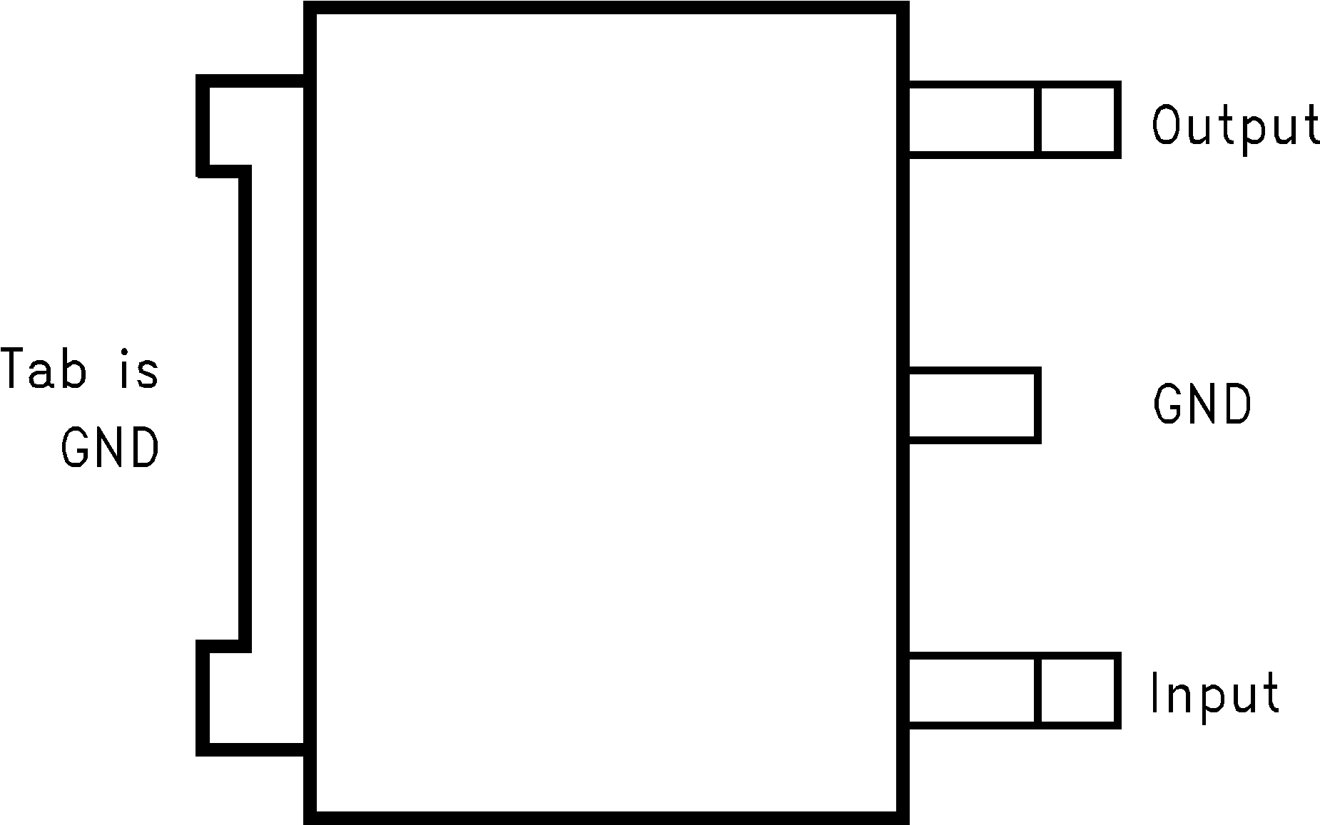
3-Pin TO-252
Top View
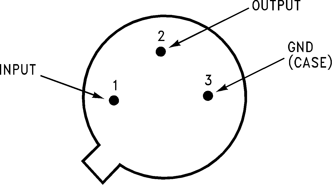
NDT Package
3-Pin TO
Top View
Pin Functions
PIN
I/O
DESCRIPTION
NAME
NO.
TO-220
TO-252
TO
GND
2/TAB
2/TAB
3
—
Tab is GND
INPUT
1
1
1
I
Input
OUTPUT
2
2
2
O
Output