JAJSDG6 June 2017 LM78M05-MIL
PRODUCTION DATA.
8 Application and Implementation
NOTE
Information in the following applications sections is not part of the TI component specification, and TI does not warrant its accuracy or completeness. TI’s customers are responsible for determining suitability of components for their purposes. Customers should validate and test their design implementation to confirm system functionality.
8.1 Application Information
The LM78M05-MIL device is a fixed voltage regulator that needs no external feedback resistors in order to set the output voltage. Input. Output capacitors are not required for the device to be stable. However, input capacitance helps filter noise from the supply and output capacitance improves the transient response.
8.2 Typical Application

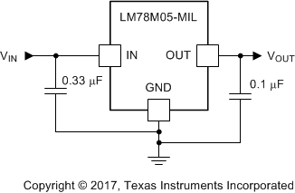
COUT is optional for improved transient response.
8.2.1 Design Requirements
For this design example, use the parameters listed in Table 1 as the input parameters.
Table 1. Design Parameters
| PARAMETER | VALUE |
|---|---|
| CIN | 0.33 µF |
| COUT | 0.1 µF |
8.2.2 Detailed Design Procedure
8.2.2.1 Input Voltage
Regardless of the output voltage option being used (5 V, 12 V, 15 V), the input voltage must be at least 2 V greater to ensure proper regulation (7 V, 14 V, 17 V).
8.2.2.2 Output Current
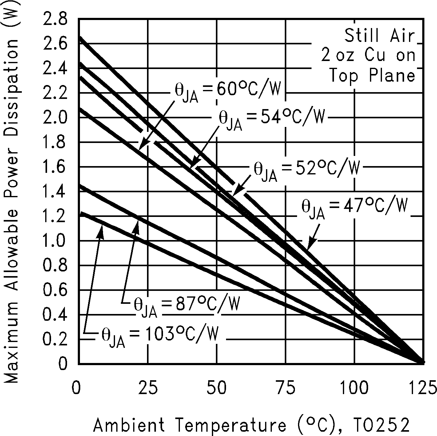
Depending on the input-output voltage differential, the output current must be limited to ensure maximum power dissipation is not exceeded. The graph in Figure 1 shows the appropriate current limit for a variety of conditions.
8.2.2.3 Input Capacitor
If no power supply filter capacitor is used or if the device is placed more than four inches away from the capacitor of the power supply, an additional capacitor placed at the input pin of the device helps bypass noise.
8.2.2.4 Output Capacitor
This device is designed to be stable with no output capacitance and can be omitted from the design if needed. However if large changes in load are expected, an output capacitor is recommended to improve the transient response.
8.2.3 Application Curves
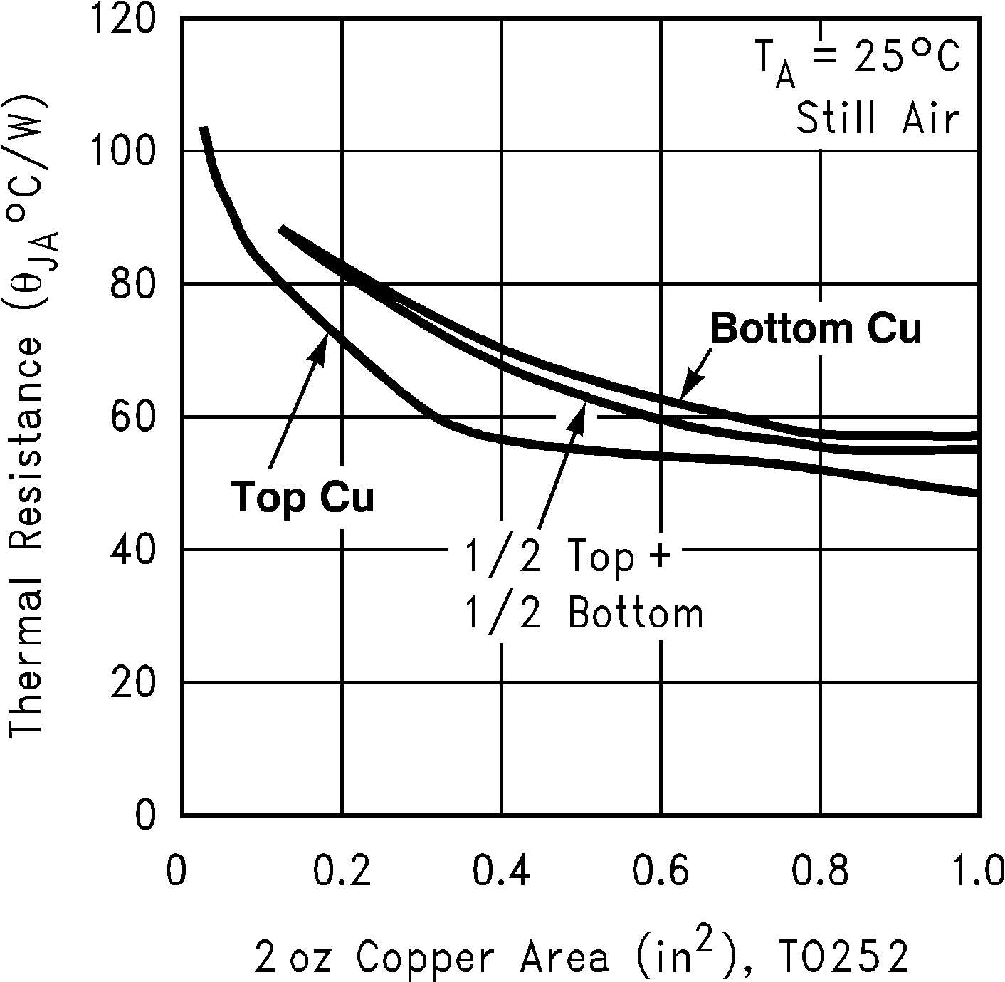
 Figure 12. RθJA vs 2-oz Copper Area for PFM
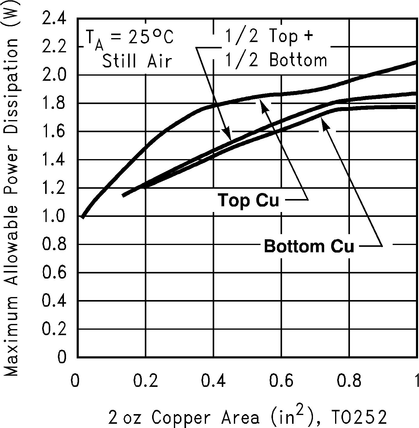
 Figure 14. Maximum Allowable Power Dissipation vs 2-oz Copper Area for PFM
 Figure 13. Maximum Allowable Power Dissipation
vs Ambient Temperature for PFM