SNAS254B October 2006 – April 2017 LM98714
PRODUCTION DATA.
- 1 Features
- 2 Applications
- 3 Description
- 4 Revision History
- 5 Pin Configuration and Functions
- 6 Specifications
-
7 Detailed Description
- 7.1 Overview
- 7.2 Functional Block Diagram
- 7.3
Feature Description
- 7.3.1 Input Clock Introduction
- 7.3.2
Modes of Operation
- 7.3.2.1 Mode 3 - Three Channel Input/Synchronous Pixel Sampling
- 7.3.2.2 Mode 2 - Two Channel Input/Synchronous Pixel Sampling
- 7.3.2.3 Mode 1a - One Channel Input/One, Two, Three, Four, or Five Color Sequential Line Sampling
- 7.3.2.4 Mode 1b - One Channel Input Per Line/Sequential Line (Input) Sampling/Three Channel Processing
- 7.3.3 Input Bias and Clamping
- 7.3.4 Coarse Pixel Phase Alignment
- 7.3.5 Internal Sample Timing
- 7.3.6 Automatic Black Level Correction Loop
- 7.3.7 Internal Timing Generation
- 7.3.8 CCD Timing Generator Master/Slave Modes
- 7.3.9 LVDS Output Mode
- 7.3.10 CMOS Output Mode
- 7.3.11 CMOS Output Data Latency Diagrams
- 7.4
Device Functional Modes
- 7.4.1 Mode 3 - Three Channel Input/Synchronous Pixel Sampling
- 7.4.2 Mode 2 - Two Channel Input/Synchronous Pixel Sampling
- 7.4.3 Mode 1a - One Channel Input/One, Two, Three, Four, Or Five Color Sequential Line Sampling
- 7.4.4 Mode 1b - One Channel Color Input Per Line/Sequential Line (Input) Sampling/Three Channel Processing
- 7.5 Programming
- 7.6 Register Maps
- 8 Application and Implementation
- 9 Device and Documentation Support
- 10Mechanical, Packaging, and Orderable Information
8 Application and Implementation
NOTE
Information in the following applications sections is not part of the TI component specification, and TI does not warrant its accuracy or completeness. TI’s customers are responsible for determining suitability of components for their purposes. Customers should validate and test their design implementation to confirm system functionality.
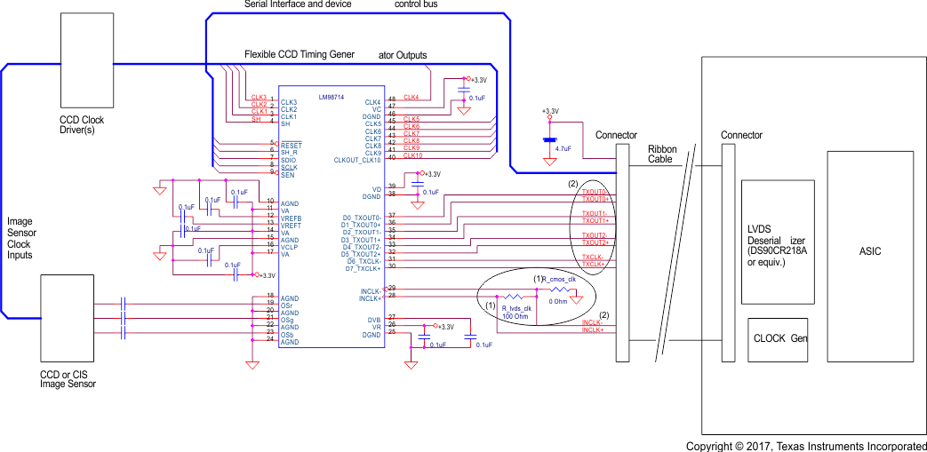
8.1 Typical Application

1. If using an LVDS input clock, terminate the clock at the pins with a 100-Ω resistor and remove the 0-Ω resistor from INCLK- to ground.
If using a CMOS input clock, short the INCLK- pin to ground and remove the 100-Ω LVDS termination resistor.
If using a CMOS input clock, short the INCLK- pin to ground and remove the 100-Ω LVDS termination resistor.
2. Maintain 100-Ω impedance for all LVDS differential pair paths.
Figure 61. Typical Application Diagram