SNAS474H April 2009 – March 2015 LM98725
PRODUCTION DATA.
- 1 Features
- 2 Applications
- 3 Description
- 4 Revision History
- 5 Pin Configuration and Functions
- 6 Specifications
-
7 Detailed Description
- 7.1 Overview
- 7.2 Functional Block Diagrams
- 7.3
Feature Description
- 7.3.1 Modes of Operation Introduction
- 7.3.2 Mode 3 - Three Channel Input/Synchronous Pixel Sampling
- 7.3.3 Mode 2 - Two Channel Input/Synchronous Pixel Sampling
- 7.3.4 Mode 1 - One Channel Input
- 7.3.5 CIS Lamp and Coefficient Modes
- 7.3.6 Clock Sources
- 7.3.7 Clock Sources - Additional Settings and Flexibility
- 7.3.8 Spread Spectrum Clock Generation (SSCG)
- 7.3.9 Typical EMI Cases and Recommended SSCG Settings
- 7.3.10 Recommended Master/Slave, Clock Source and SSCG Combinations and Settings
- 7.4
Device Functional Modes
- 7.4.1 Mode 3 - Three Channel Input/Synchronous Pixel Sampling
- 7.4.2 Mode 2 - Two Channel Input/Synchronous Pixel Sampling
- 7.4.3 Mode 1 - One Channel Input
- 7.4.4 Input Bias and Clamping
- 7.4.5 Sample/Hold Mode
- 7.4.6 DC Coupled Applications
- 7.4.7 Input Source Follower Buffers
- 7.4.8 CDS Mode
- 7.4.9 VCLP DAC
- 7.4.10 Gain and Offset Correction
- 7.4.11 LM98725 Typical Line Timing and Pixel Gain Regions
- 7.4.12
Automatic Black and White Level Calibration Loops
- 7.4.12.1 Calibration Overview
- 7.4.12.2 Different Modes for Different Needs
- 7.4.12.3 Calibration Initiation
- 7.4.12.4 Key Calibration Settings
- 7.4.12.5 General Black Loop Operation
- 7.4.12.6 ADAC/DDAC Convergence
- 7.4.12.7 General White Loop Operation
- 7.4.12.8 White Loop Modes
- 7.4.12.9 Bimodal (Automatic) Correction
- 7.4.13 Coarse Pixel Phase Alignment
- 7.4.14 Internal Sample Timing
- 7.4.15 CCD Timing Generator Master/Slave Modes
- 7.4.16 LVDS Control Bit Coding - LM98714 Mode
- 7.4.17 Flexible LVDS Formatting Mode: Mapping
- 7.4.18 LVDS Data Randomization for EMI Reduction
- 7.4.19 LVDS Drive Strength Adjust
- 7.4.20 LVDS Output Timing Details
- 7.4.21 LVDS Data Latency Diagrams
- 7.4.22 Data Test Patterns
- 7.4.23 CMOS Output Format
- 7.4.24 CMOS Output Data Latency Diagrams
- 7.4.25 Serial Interface
- 7.5 Register Maps
- 8 Layout
- 9 Device and Documentation Support
- 10Mechanical, Packaging, and Orderable Information
1 Features
- LVDS/CMOS Outputs
- LVDS/CMOS/Crystal Clock Source with PLL Multiplication
- Integrated Flexible Spread Spectrum Clock Generation
- CDS or S/H Processing for CCD or CIS Sensors
- Independent Gain/Offset Correction for Each Channel
- Automatic per-Channel Gain and Offset Calibration
- Programmable Input Clamp Voltage
- Flexible CCD/CIS Sensor Timing Generator
2 Applications
- Multi-Function Peripherals
- High-speed Currency/Check Scanners
- Flatbed or Handheld Color Scanners
- High-speed Document Scanners
-
Key Specifications:
- Maximum Input Level
- 1.2 or 2.4 Volt Modes
- (Both with + or - Polarity Option)
- ADC Resolution: 16-Bit
- ADC Sampling Rate: 81 MSPS
- INL: +17/- 28 LSB (typ)
- Channel Sampling Rate: 30/30/27 MSPS
- PGA Gain Steps: 256 Steps
- PGA Gain Range: 0.62 to 8.3x
- Analog DAC Resolution: ±9 Bits
- Analog DAC Range: ±307 mV or ±614 mV
- Digital DAC Resolution: ±6 Bits
- Digital DAC Range: -2048 LSB to + 2016 LSB
- SNR: –74dB (@0 dB PGA Gain)
- Power Dissipation: 755 mW (LVDS)
- Operating Temp: 0 to 70°C
- Supply Voltage: 3.3 V Nominal (3.0-V to 3.6-V Range)
- Maximum Input Level
3 Description
The LM98725 is a fully integrated, high performance 16-Bit, 81 MSPS signal processing solution for digital color copiers, scanners, and other image processing applications. The LM98725 achieves high-speed signal throughput with an innovative architecture utilizing Correlated Double Sampling (CDS), typically employed with CCD arrays, or Sample and Hold (S/H) inputs (for higher speed CCD or CMOS image sensors). The signal paths utilize 8 bit Programmable Gain Amplifiers (PGA), a ±9-Bit offset correction DAC, and independently controlled Digital Black Level correction loops for each input. The independently programmed PGA and offset DAC allow unique values of gain and offset for each of the three analog inputs. The signals are then routed to a 81 MHz high performance analog-to-digital converter (ADC). The fully differential processing channel shows exceptional noise immunity with a very low noise floor of –74 dB. The 16-bit ADC has excellent dynamic performance making the LM98725 transparent in the image reproduction chain.
A very flexible integrated Spread Spectrum Clock Generation (SSCG) modulator is included to assist with EM compliance and reduce system costs.
Device Information(1)
| PART NUMBER | PACKAGE | BODY SIZE (NOM) |
|---|---|---|
| LM98725 | TSSOP (56) | 14.0 mm × 6.10 mm |
- For all available packages, see the orderable addendum at the end of the datasheet.
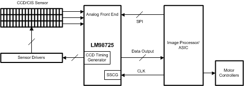
System Block Diagram

4 Revision History
Changes from G Revision (October 2014) to H Revision
- Changed "29" to "33" for Pin number 32 in Pin FunctionsGo
- Deleted "Boldface limits apply..." statement in Electrical Characteristics and AC Timing SpecificationsGo
- Changed "internal" to "external" and "external" to "internal" for "SH_R Capture Clock Select (Page 0, Register 0x00, Bit 5)" heading in Clock Sources - Additional Settings and FlexibilityGo
- Changed 25 MHz to 27 MHz and 75 MHz to 81 MHz for Table 3Go
- Changed "Page 2" to "Page 0" in CCD Timing Generator Master/Slave ModesGo
- Changed "Page 2" to "Page 0" in Master Timing Generator ModeGo
- Changed "1100 0000" to " 1100 0010" in Table 18Go
Changes from F Revision (January 2014) to G Revision
- Added, updated, or renamed the following sections: Device Information Table, Pin Configuration and Functions; Layout; Device and Documentation Support; Mechanical, Packaging, and Ordering Information Go
- Added "Note" in Serial InterfaceGo
Changes from E Revision (April 2013) to F Revision
- Added content from System Overview section to end of document. Go
Changes from D Revision (April 2009) to E Revision
- Changed layout of National Data Sheet to TI formatGo