SNOSBY1C June   1999  – December 2015 LMC567

PRODUCTION DATA.  

  1. Features
  2. Applications
  3. Description
  4. Revision History
  5. Device Comparison Table
  6. Pin Configuration and Functions
  7. Specifications
    1. 7.1 Absolute Maximum Ratings
    2. 7.2 Recommended Operating Conditions
    3. 7.3 Thermal Information
    4. 7.4 Electrical Characteristics
    5. 7.5 Typical Characteristics
  8. Parameter Measurement Information
    1. 8.1 Test Circuit
  9. Detailed Description
    1. 9.1 Overview
    2. 9.2 Functional Block Diagram
    3. 9.3 Feature Description
      1. 9.3.1 Oscillator
      2. 9.3.2 Input
      3. 9.3.3 Loop Filter
      4. 9.3.4 Output Filter
      5. 9.3.5 Output
    4. 9.4 Device Functional Modes
      1. 9.4.1 Operation as LM567
  10. 10Application and Implementation
    1. 10.1 Application Information
    2. 10.2 Typical Application
      1. 10.2.1 Design Requirements
      2. 10.2.2 Detailed Design Procedure
        1. 10.2.2.1 Timing Components
        2. 10.2.2.2 Bandwidth
        3. 10.2.2.3 Output Filter
        4. 10.2.2.4 Supply Decoupling
      3. 10.2.3 Application Curve
  11. 11Power Supply Recommendations
  12. 12Layout
    1. 12.1 Layout Guidelines
    2. 12.2 Layout Example
  13. 13Device and Documentation Support
    1. 13.1 Device Support
      1. 13.1.1 Development Support
    2. 13.2 Community Resources
    3. 13.3 Trademarks
    4. 13.4 Electrostatic Discharge Caution
    5. 13.5 Glossary
  14. 14Mechanical, Packaging, and Orderable Information

パッケージ・オプション

メカニカル・データ(パッケージ|ピン)
サーマルパッド・メカニカル・データ

8 Parameter Measurement Information

All parameters are measured according to the conditions described in Specifications.

8.1 Test Circuit

Figure 7 was used to make the measurements of the typical characteristics of the LMC567.
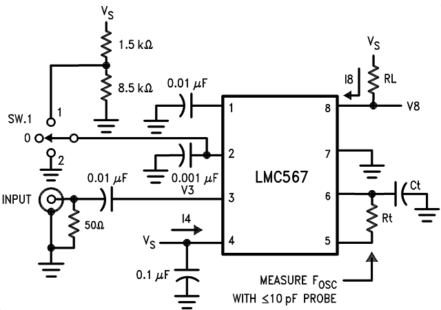
LMC567 00867002.png Figure 7. LMC567 Test Circuit

Table 1. Rt and Ct Values for the Test Circuit

RtCt Rt Ct
#1 100k 300 pF
#2 10k 300 pF
#3 5.1k 62 pF