JAJS910H January 2000 – December 2024 LMC6035 , LMC6036
PRODUCTION DATA
- 1
- 1 特長
- 2 アプリケーション
- 3 概要
- 4 Pin Configuration and Functions
- 5 Specifications
- 6 Detailed Description
- 7 Application and Implementation
- 8 Device and Documentation Support
- 9 Revision History
- 10Mechanical, Packaging, and Orderable Information
パッケージ・オプション
メカニカル・データ(パッケージ|ピン)
サーマルパッド・メカニカル・データ
発注情報
7.2.1 Differential Driver
The LMC603x are an excellent choice for low-voltage applications. A desirable feature that the LMC603x bring to low-voltage applications is the output drive capability—a hallmark for TI's CMOS amplifiers. The circuit of Figure 7-3 illustrates the drive capability of the LMC603x at 3V of supply. These devices are used as a differential output driver for a one-to-one audio transformer, like those used for isolating ground from the telephone lines. The transformer (T1) loads the op amps with about 600Ω of ac load, at 1kHz. Capacitor C1 functions to block dc from the low winding resistance of T1. Although the value of C1 is relatively high, the capacitive load reactance (XC) is negligible compared to inductive reactance (XI) of T1.
 Figure 7-3 Differential Driver
The circuit in Figure 7-3 consists of one input signal and two output signals. U1A amplifies the input with an inverting gain of −2, while the U1B amplifies the input with a non-inverting gain of +2. The two outputs are 180° out of phase with each other; therefore, the gain across the differential output is 4. As the differential output swings between the supply rails, one of the op amps sources the current to the load, while the other op amp sinks the current.
How good a CMOS op amp can sink or source a current is an important factor in determining output swing capability. The output stage of the LMC603x—like many op amps—sources and sinks output current through two complementary transistors in series. This totem pole arrangement translates to a channel resistance (Rdson) at each supply rail that acts to limit the output swing. Most CMOS op amps are able to swing the outputs very close to the rails; except, however, under the difficult conditions of low supply voltage and heavy load. The LMC603x exhibit exceptional output swing capability under these conditions.
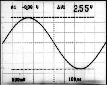
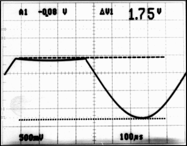
The scope photos of Figure 7-4 and Figure 7-5 represent measurements taken directly at the output (relative to GND) of U1A, in Figure 7-3. Figure 7-4 illustrates the output swing capability of the LMC6035, while Figure 7-5 provides a benchmark comparison. (The benchmark op amp is another low-voltage (3V) op amp manufactured by one of our reputable competitors.)
 Figure 7-4 Output Swing Performance of the LMC6035 per the Circuit of Figure 7-3
 Figure 7-5 Output Swing Performance of
Benchmark Op Amp per the Circuit of Figure 7-3
Notice the excellent drive capability of LMC6035 when compared with the benchmark measurement—even though the benchmark op amp uses twice the supply current.
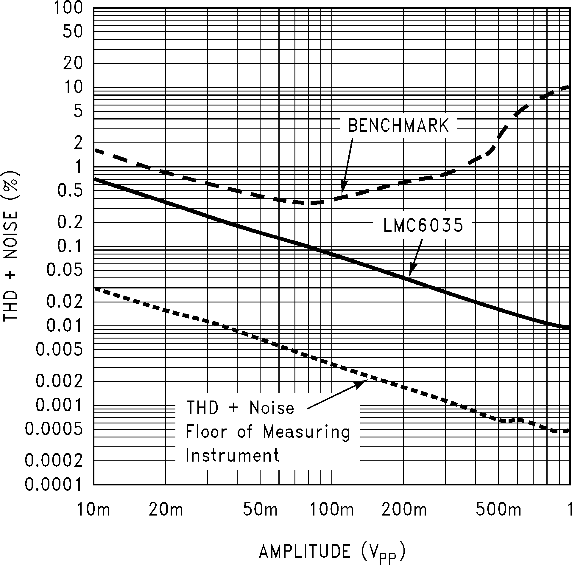
Not only does the LMC603x provide excellent output swing capability at low supply voltages, but these devices also maintain high open-loop gain (A OL) with heavy loads. To illustrate this, the LMC6035 and the benchmark op amp were compared for distortion performance in the circuit of Figure 7-3. Figure 7-6 shows this comparison. The y-axis represents percent total harmonic distortion (THD + noise) across the loaded secondary of T1. The x-axis represents the input amplitude of a 1kHz sine wave. (Notice that T1 loses about 20% of the voltage to the voltage divider of RL (600Ω) and T1 winding resistances—a performance deficiency of the transformer.)
 Figure 7-6 THD+Noise Performance of LMC6035 and Benchmark per Circuit of Figure 7-3
Figure 7-6 shows the excellent distortion performance of the LMC603x over that of the benchmark op amp. The heavy loading of the circuit causes the AOL of the benchmark part to drop significantly, which causes increased distortion.