JAJSIG5C May 2019 – December 2024 LMG1025-Q1
PRODUCTION DATA
- 1
- 1 特長
- 2 アプリケーション
- 3 概要
- 4 Pin Configuration and Functions
- 5 Specifications
- 6 Detailed Description
- 7 Application and Implementation
- 8 Power Supply Recommendations
- 9 Layout
- 10Device and Documentation Support
- 11Revision History
- 12Mechanical, Packaging, and Orderable Information
デバイスごとのパッケージ図は、PDF版データシートをご参照ください。
メカニカル・データ(パッケージ|ピン)
- DEE|6
サーマルパッド・メカニカル・データ
4 Pin Configuration and Functions
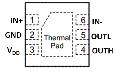
 Figure 4-1 DEE6-Pin WSONTop View
 Figure 4-2 DRV6-Pin WSONTop View
Table 4-1 Pin Functions
| PIN | I/O(1) | DESCRIPTION | |
|---|---|---|---|
| NAME | NO. | ||
| GND | 2 | G | Power supply and source return. Connect with a direct path to the transistor’s source. |
| IN+ | 1 | I | Positive logic-level input. |
| IN– | 6 | I | Negative logic-level input. |
| OUTL | 5 | O | Pull-down gate drive output. Connect through an optional resistor to the target transistor’s gate. |
| OUTH | 4 | O | Pull-up gate drive output. Connect through a resistor to the target transistor’s gate. |
| VDD | 3 | P | Input voltage supply. Decouple through a compact capacitor to GND. |
| Thermal Pad | - | - | Internally connected to GND through substrate. Connect this pad to large copper area, generally a ground plane. |
(1) I=Input, O=Output, P=Power, G=Ground