JAJSIG5C May 2019 – December 2024 LMG1025-Q1
PRODUCTION DATA
- 1
- 1 特長
- 2 アプリケーション
- 3 概要
- 4 Pin Configuration and Functions
- 5 Specifications
- 6 Detailed Description
- 7 Application and Implementation
- 8 Power Supply Recommendations
- 9 Layout
- 10Device and Documentation Support
- 11Revision History
- 12Mechanical, Packaging, and Orderable Information
デバイスごとのパッケージ図は、PDF版データシートをご参照ください。
メカニカル・データ(パッケージ|ピン)
- DEE|6
サーマルパッド・メカニカル・データ
7.2.2.2 Creating Nanosecond Pulse
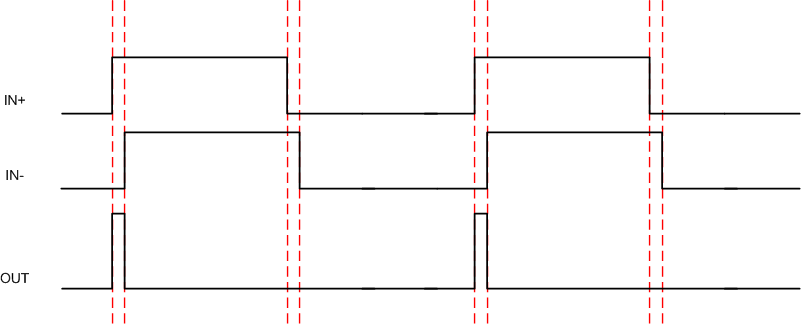
LMG1025-Q1 can be used to drive pulses of nano seconds duration on to a capacitive load. LMG1025-Q1 can be driven with a equivalently short pulse on one input pin. However, this takes a sufficiently strong digital driver and careful consideration of the routing parasitics from digital output to input of LMG1025-Q1. Two inputs and included AND gate in LMG1025-Q1 provide an alternate method to create a short pulse at the LMG1025-Q1 output. Starting with both IN+ and IN– at low, taking IN+ high will cause the output to go high. Now if IN– is taken high as well, output will be pulled low. So a digital signal and its delayed version can be applied to IN+ and IN– respectively to create a pulse at the output with width corresponding to the delay between the signals, as shown in Figure 7-5. The delay can be digitally controlled in the nanosecond range. This method alleviates the requirements for driving the input of LMG1025-Q1. If a separate delayed version of the digital signal is not available, an RC delay followed by a buffer can be used to derive the second signal. Optionally, if LMG1025-Q1 must be driven with a single short duration pulse, that pulse can itself be generated using another LMG1025-Q1 by the above method to meet drive requirements.
 Figure 7-5 Timing Diagram To Create Short Pulses