JAJSIG5C May 2019 – December 2024 LMG1025-Q1
PRODUCTION DATA
- 1
- 1 特長
- 2 アプリケーション
- 3 概要
- 4 Pin Configuration and Functions
- 5 Specifications
- 6 Detailed Description
- 7 Application and Implementation
- 8 Power Supply Recommendations
- 9 Layout
- 10Device and Documentation Support
- 11Revision History
- 12Mechanical, Packaging, and Orderable Information
パッケージ・オプション
デバイスごとのパッケージ図は、PDF版データシートをご参照ください。
メカニカル・データ(パッケージ|ピン)
- DRV|6
- DEE|6
サーマルパッド・メカニカル・データ
- DRV|6
発注情報
7.2.3 Application Curves
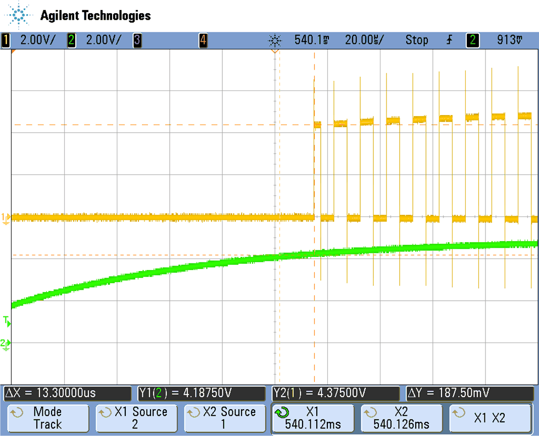
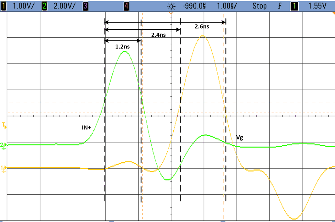
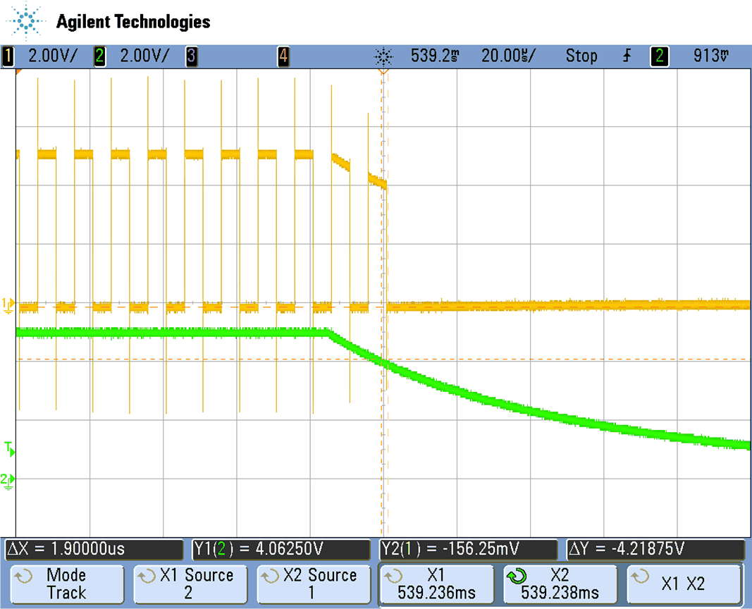
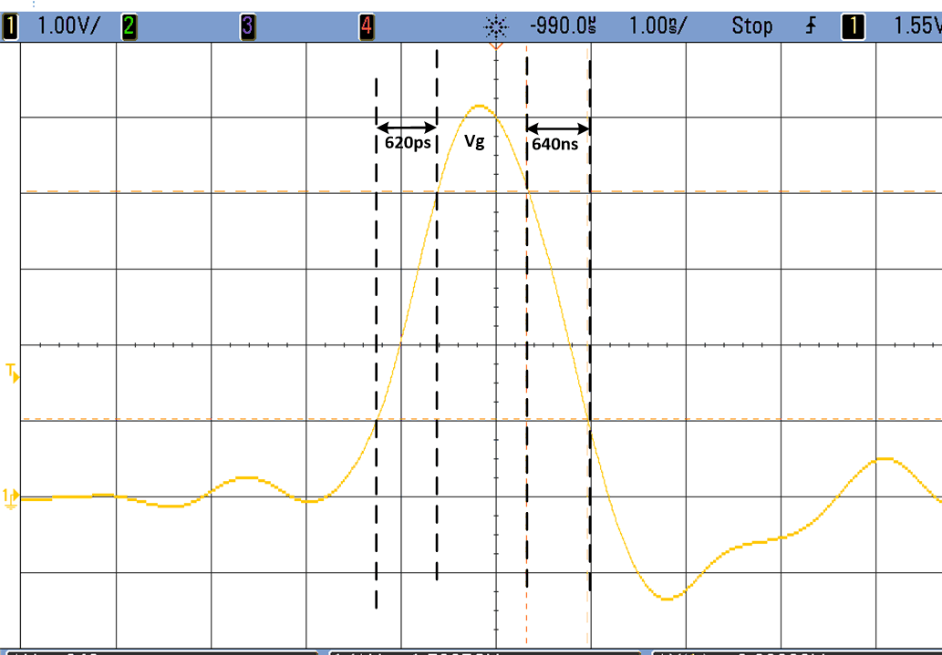
LMG1025-Q1 EVM is used to take application waveforms. This EVM has LDO, input buffer, GaN FET, and load resistor. It shows the switching performance of the LMG1025-Q1 when equivalent laser diode current is switched. Figure 7-6 and Figure 7-7 show VDD turn-on and turn-off delay in an application-like set-up. System designer need to make sure that these delays are acceptable in their designs. LIDAR design needs to pulse the laser diode for very short duration. Figure 7-8 shows how LMG1025-Q1 can not only handle nano-second pulse at its input but also can produce a nano-second pulse at the output while driving a reasonably sized GaN FET that has 3.2nC of typical total gate charge. Figure 7-8 also shows very small, e.g. less than 3 ns, rising and falling propagation delay of LMG1025-Q1. Figure 7-9 shows drive strength of LMG1025-Q1. It shows how LMG1025-Q1 can achieve sub-nano second rise and fall time, which is very important for LIDAR applicatoins.
 Figure 7-6 Startup Time
 Figure 7-8 Input Pulse Width and
Propagation Delays
 Figure 7-7 Shutdown Time
 Figure 7-9 Rise and Fall
Time