JAJSLK5B October   2020  – May 2022 LMG3422R050 , LMG3425R050

PRODUCTION DATA  

  1. 特長
  2. アプリケーション
  3. 概要
  4. Revision History
  5. Device Comparison
  6. Pin Configuration and Functions
  7. Specifications
    1. 7.1 Absolute Maximum Ratings
    2. 7.2 ESD Ratings
    3. 7.3 Recommended Operating Conditions
    4. 7.4 Thermal Information
    5. 7.5 Electrical Characteristics
    6. 7.6 Switching Characteristics
    7. 7.7 Typical Characteristics
  8. Parameter Measurement Information
    1. 8.1 Switching Parameters
      1. 8.1.1 Turn-On Times
      2. 8.1.2 Turn-Off Times
      3. 8.1.3 Drain-Source Turn-On Slew Rate
      4. 8.1.4 Turn-On and Turn-Off Switching Energy
  9. Detailed Description
    1. 9.1 Overview
    2. 9.2 Functional Block Diagram
    3. 9.3 Feature Description
      1. 9.3.1  GaN FET Operation Definitions
      2. 9.3.2  Direct-Drive GaN Architecture
      3. 9.3.3  Drain-Source Voltage Capability
      4. 9.3.4  Internal Buck-Boost DC-DC Converter
      5. 9.3.5  VDD Bias Supply
      6. 9.3.6  Auxiliary LDO
      7. 9.3.7  Fault Detection
        1. 9.3.7.1 Overcurrent Protection and Short-Circuit Protection
        2. 9.3.7.2 Overtemperature Shutdown
        3. 9.3.7.3 UVLO Protection
        4. 9.3.7.4 Fault Reporting
      8. 9.3.8  Drive Strength Adjustment
      9. 9.3.9  Temperature-Sensing Output
      10. 9.3.10 Ideal-Diode Mode Operation
    4. 9.4 Start Up Sequence
    5. 9.5 Safe Operation Area (SOA)
      1. 9.5.1 Safe Operation Area (SOA) - Repetitive SOA
    6. 9.6 Device Functional Modes
  10. 10Application and Implementation
    1. 10.1 Application Information
    2. 10.2 Typical Application
      1. 10.2.1 Design Requirements
      2. 10.2.2 Detailed Design Procedure
        1. 10.2.2.1 Slew Rate Selection
          1. 10.2.2.1.1 Start-Up and Slew Rate With Bootstrap High-Side Supply
        2. 10.2.2.2 Signal Level-Shifting
        3. 10.2.2.3 Buck-Boost Converter Design
      3. 10.2.3 Application Curves
    3. 10.3 Do's and Don'ts
  11. 11Power Supply Recommendations
    1. 11.1 Using an Isolated Power Supply
    2. 11.2 Using a Bootstrap Diode
      1. 11.2.1 Diode Selection
      2. 11.2.2 Managing the Bootstrap Voltage
  12. 12Layout
    1. 12.1 Layout Guidelines
      1. 12.1.1 Solder-Joint Reliability
      2. 12.1.2 Power-Loop Inductance
      3. 12.1.3 Signal-Ground Connection
      4. 12.1.4 Bypass Capacitors
      5. 12.1.5 Switch-Node Capacitance
      6. 12.1.6 Signal Integrity
      7. 12.1.7 High-Voltage Spacing
      8. 12.1.8 Thermal Recommendations
    2. 12.2 Layout Examples
  13. 13Device and Documentation Support
    1. 13.1 Documentation Support
      1. 13.1.1 Related Documentation
    2. 13.2 Receiving Notification of Documentation Updates
    3. 13.3 サポート・リソース
    4. 13.4 Trademarks
    5. 13.5 Electrostatic Discharge Caution
    6. 13.6 Export Control Notice
    7. 13.7 Glossary
  14. 14Mechanical, Packaging, and Orderable Information

パッケージ・オプション

メカニカル・データ(パッケージ|ピン)
  • RQZ|54
サーマルパッド・メカニカル・データ
発注情報

Switching Parameters

Figure 8-1 shows the circuit used to measure most switching parameters. The top device in this circuit is used to re-circulate the inductor current and functions in third-quadrant mode only. Only the LMG3422R050 must be used as the top device as it does not have the ideal-diode mode feature. Do not use the LMG3425R050 for the top device. If the top device has the ideal-diode mode feature, it will automatically turn on the GaN FET when the inductor current is re-circulating and cause a shoot-through current event when the bottom device turns on. The bottom device is the active device that turns on to increase the inductor current to the desired test current. The bottom device is then turned off and on to create switching waveforms at a specific inductor current. Both the drain current (at the source) and the drain-source voltage is measured. Figure 8-2 shows the specific timing measurement. TI recommends to use the half-bridge as double pulse tester. Excessive third-quadrant operation can overheat the top device.
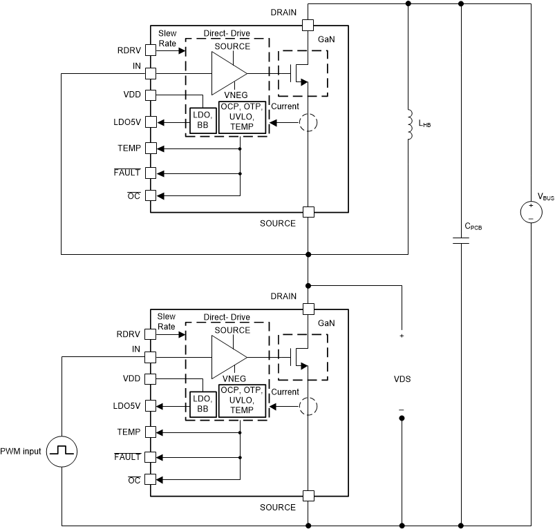
GUID-2F1DC697-999F-4634-89E8-630E16238191-low.gifFigure 8-1 Circuit Used to Determine Switching Parameters
Figure 8-2 Measurement to Determine Propagation Delays and Slew Rates