JAJSI48C March 2017 – October 2019 LMH1228
PRODUCTION DATA.
- 1 特長
- 2 アプリケーション
- 3 概要
- 4 改訂履歴
- 5 Pin Configuration and Functions
- 6 Specifications
-
7 Detailed Description
- 7.1 Overview
- 7.2 Functional Block Diagram
- 7.3
Feature Description
- 7.3.1 4-Level Input Pins and Thresholds
- 7.3.2 OUT0_SEL and SDI_OUT2_SEL Control
- 7.3.3 Input Signal Detect
- 7.3.4 Continuous Time Linear Equalizer (CTLE)
- 7.3.5 Clock and Data (CDR) Recovery
- 7.3.6 Internal Eye Opening Monitor (EOM)
- 7.3.7 Output Function Control
- 7.3.8 Output Driver Control
- 7.3.9 Status Indicators and Interrupts
- 7.4 Device Functional Modes
- 7.5 Register Maps
- 8 Application and Implementation
- 9 Power Supply Recommendations
- 10Layout
- 11デバイスおよびドキュメントのサポート
- 12メカニカル、パッケージ、および注文情報
パッケージ・オプション
メカニカル・データ(パッケージ|ピン)
- RTV|32
サーマルパッド・メカニカル・データ
- RTV|32
発注情報
8.2.1.3 Application Curves
The LMH1228 performance on SDI_OUT1+ and SDI_OUT2+ was measured with the test setups shown in Figure 22 and Figure 23.
 Figure 22. Test Setup for LMH1228 to SDI_OUT1+
  Figure 23. Test Setup for LMH1228 to SDI_OUT2+
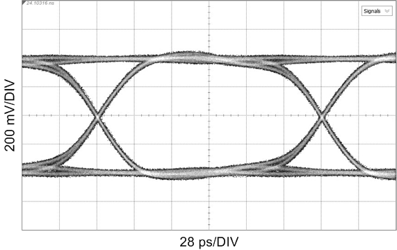
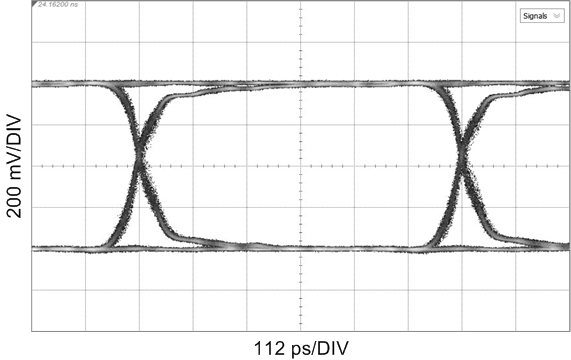
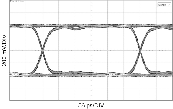
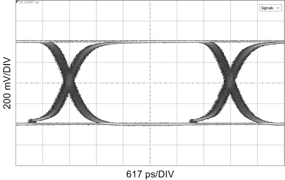
 The eye diagrams in this subsection show how the LMH1228 improves overall signal integrity in the data path for 100-Ω differential FR4 PCB trace at IN0±.

Measured at SDI_OUT1+
HOST_EQ0 = F, SDI_OUT2_SEL = L, OUT_CTRL = F
Figure 24. 11.88 Gbps, TL = 20" FR4, Reclocked HOST_EQ0 = F, SDI_OUT2_SEL = L, OUT_CTRL = F

Measured at SDI_OUT1+
HOST_EQ0 = F, SDI_OUT2_SEL = L, OUT_CTRL = F
Figure 26. 5.94 Gbps, TL = 20" FR4, Reclocked HOST_EQ0 = F, SDI_OUT2_SEL = L, OUT_CTRL = F

Measured at SDI_OUT1+
HOST_EQ0 = F, SDI_OUT2_SEL = L, OUT_CTRL = F
Figure 28. 2.97 Gbps, TL = 20" FR4, Reclocked HOST_EQ0 = F, SDI_OUT2_SEL = L, OUT_CTRL = F

Measured at SDI_OUT1+
HOST_EQ0 = F, SDI_OUT2_SEL = L, OUT_CTRL = F
Figure 30. 1.485 Gbps, TL = 20" FR4, Reclocked HOST_EQ0 = F, SDI_OUT2_SEL = L, OUT_CTRL = F

Measured at SDI_OUT1+
HOST_EQ0 = F, SDI_OUT2_SEL = L, OUT_CTRL = F
Figure 32. 270 Mbps, TL = 20" FR4, Reclocked HOST_EQ0 = F, SDI_OUT2_SEL = L, OUT_CTRL = F

Measured at SDI_OUT2+
HOST_EQ0 = F, SDI_OUT2_SEL = L, OUT_CTRL = F
Figure 25. 11.88 Gbps, TL = 20" FR4, Reclocked HOST_EQ0 = F, SDI_OUT2_SEL = L, OUT_CTRL = F

Measured at SDI_OUT2+
HOST_EQ0 = F, SDI_OUT2_SEL = L, OUT_CTRL = F
Figure 27. 5.94 Gbps, TL = 20" FR4, Reclocked HOST_EQ0 = F, SDI_OUT2_SEL = L, OUT_CTRL = F

Measured at SDI_OUT2+
HOST_EQ0 = F, SDI_OUT2_SEL = L, OUT_CTRL = F
Figure 29. 2.97 Gbps, TL = 20" FR4, Reclocked HOST_EQ0 = F, SDI_OUT2_SEL = L, OUT_CTRL = F

Measured at SDI_OUT2+
HOST_EQ0 = F, SDI_OUT2_SEL = L, OUT_CTRL = F
Figure 31. 1.485 Gbps, TL = 20" FR4, Reclocked HOST_EQ0 = F, SDI_OUT2_SEL = L, OUT_CTRL = F

Measured at SDI_OUT2+
HOST_EQ0 = F, SDI_OUT2_SEL = L, OUT_CTRL = F
Figure 33. 270 Mbps, TL = 20" FR4, Reclocked HOST_EQ0 = F, SDI_OUT2_SEL = L, OUT_CTRL = F