JAJSJ18A June   2024  – October 2024 LMH1229 , LMH1239

PRODUCTION DATA  

  1.   1
  2. 特長
  3. アプリケーション
  4. 概要
  5. Pin Configuration and Functions
  6. Specifications
    1. 5.1 Absolute Maximum Ratings
    2. 5.2 ESD Ratings
    3. 5.3 Recommended Operating Conditions
    4. 5.4 Thermal Information
    5. 5.5 Electrical Characteristics
    6. 5.6 Timing Requirements for Serial Management (SM) Bus Interface
    7. 5.7 Timing Requirements for Serial Parallel Interface (SPI) Interface
    8. 5.8 Typical Characteristics
      1. 5.8.1 TX Characteristics
      2. 5.8.2 RX Characteristics
  7. Detailed Description
    1. 6.1 Overview
    2. 6.2 Functional Block Diagram
    3. 6.3 Feature Description
      1. 6.3.1 4-Level Input Pins and Thresholds
      2. 6.3.2 Input and Output Signal Flow Control
        1. 6.3.2.1 Input Mux Selection (LMH1239 Only)
        2. 6.3.2.2 Output Mux and SDI_OUT Selection
      3. 6.3.3 Input Carrier Detect
      4. 6.3.4 Adaptive Cable Equalizer (SDI_IN±, SDI_IN1±)
      5. 6.3.5 Clock and Data (CDR) Recovery
      6. 6.3.6 CDR Loop Bandwidth Control
      7. 6.3.7 Output Function Control
      8. 6.3.8 Output Driver Control
        1. 6.3.8.1 Line-Side 75Ω Output Cable Driver (SDI_OUT±)
          1. 6.3.8.1.1 Output Amplitude (VOD)
          2. 6.3.8.1.2 Output Pre-Emphasis
          3. 6.3.8.1.3 Output Slew Rate
          4. 6.3.8.1.4 Output Polarity Inversion
        2. 6.3.8.2 Host-Side 100Ω Output Driver (OUT0±, OUT1±)
      9. 6.3.9 Debug and Diagnostic Features
        1. 6.3.9.1 Internal Eye Opening Monitor (EOM)
        2. 6.3.9.2 PRBS Generator, Error Checker, and Error Injector
        3. 6.3.9.3 Status Indicators and Interrupts
          1. 6.3.9.3.1 LOCK_N (Lock Indicator)
          2. 6.3.9.3.2 CD_N (Carrier Detect)
          3. 6.3.9.3.3 Cable Fault Detection (SDI_OUT+ Only)
          4. 6.3.9.3.4 INT_N (Interrupt)
        4. 6.3.9.4 Additional Programmability
          1. 6.3.9.4.1 Cable EQ Index (CEI)
          2. 6.3.9.4.2 Digital MUTEREF
    4. 6.4 Device Functional Modes
      1. 6.4.1 System Management Bus (SMBus) Mode
        1. 6.4.1.1 SMBus Read and Write Transaction
          1. 6.4.1.1.1 SMBus Write Operation Format
          2. 6.4.1.1.2 SMBus Read Operation Format
      2. 6.4.2 Serial Peripheral Interface (SPI) Mode
        1. 6.4.2.1 SPI Read and Write Transactions
          1. 6.4.2.1.1 SPI Write Transaction Format
          2. 6.4.2.1.2 SPI Read Transaction Format
        2. 6.4.2.2 SPI Daisy Chain
  8. Application and Implementation
    1. 7.1 Application Information
      1. 7.1.1 SMPTE Requirements and Specifications
      2. 7.1.2 Optimizing the Time to Adapt and Lock
      3. 7.1.3 Optimized Loop Bandwidth Settings for Diagnostic or Cascade Applications
      4. 7.1.4 LMH1229 and LMH1297 (EQ Mode) Pin-to-Pin Compatibility
    2. 7.2 Typical Application
      1. 7.2.1 Cable Equalizer With Loop-Through
        1. 7.2.1.1 Design Requirements
        2. 7.2.1.2 Detailed Design Procedure
        3. 7.2.1.3 Application Curves
      2. 7.2.2 Cable Equalizer With Redundant SDI Input (LMH1239 only)
        1. 7.2.2.1 Design Requirements
        2. 7.2.2.2 Detailed Design Procedure
        3. 7.2.2.3 Application Curves
    3. 7.3 Power Supply Recommendations
    4. 7.4 Layout
      1. 7.4.1 Layout Guidelines
        1. 7.4.1.1 Board Stack-Up and Ground References
        2. 7.4.1.2 High-Speed PCB Trace Routing and Coupling
          1. 7.4.1.2.1 SDI_IN± and SDI_OUT±:
          2. 7.4.1.2.2 OUT0± and OUT1±:
        3. 7.4.1.3 Anti-Pads
        4. 7.4.1.4 BNC Connector Layout and Routing
        5. 7.4.1.5 Power Supply and Ground Connections
        6. 7.4.1.6 Footprint Recommendations
      2. 7.4.2 Layout Example
  9. Device and Documentation Support
    1. 8.1 Documentation Support
      1. 8.1.1 Related Documentation
    2. 8.2 ドキュメントの更新通知を受け取る方法
    3. 8.3 サポート・リソース
    4. 8.4 Trademarks
    5. 8.5 静電気放電に関する注意事項
    6. 8.6 用語集
  10. Revision History
  11. 10Mechanical, Packaging, and Orderable Information

パッケージ・オプション

メカニカル・データ(パッケージ|ピン)
サーマルパッド・メカニカル・データ
発注情報

Application Curves

The LMH12x9 output eye performance was measured with the test setups shown in Figure 7-4 and Figure 7-5.

LMH1229 LMH1239 Test Setup for
            LMH12x9 PCB Output (OUT0±, OUT1±) Figure 7-4 Test Setup for LMH12x9 PCB Output (OUT0±, OUT1±)
LMH1229 LMH1239 Test Setup for
            LMH12x9 Loop-Through (SDI_OUT+) Figure 7-5 Test Setup for LMH12x9 Loop-Through (SDI_OUT+)

The eye diagrams measured on the LMH1239EVM in this subsection show the LMH12x9 100Ω differential PCB output at OUT0± and OUT1± (Figure 7-7 - Figure 7-8) and LMH12x9 75Ω loop-through cable output at SDI_OUT+ (Figure 7-9).

Additionally, LMH12x9 BER (bit error rate) performance was measured with the test setup shown in Figure 7-6. Phabrix Qx BER results on the LMH1239EVM are shown in Figure 7-10.

LMH1229 LMH1239 Test Setup for
            LMH12x9 BER Performance (OUT0±) Figure 7-6 Test Setup for LMH12x9 BER Performance (OUT0±)
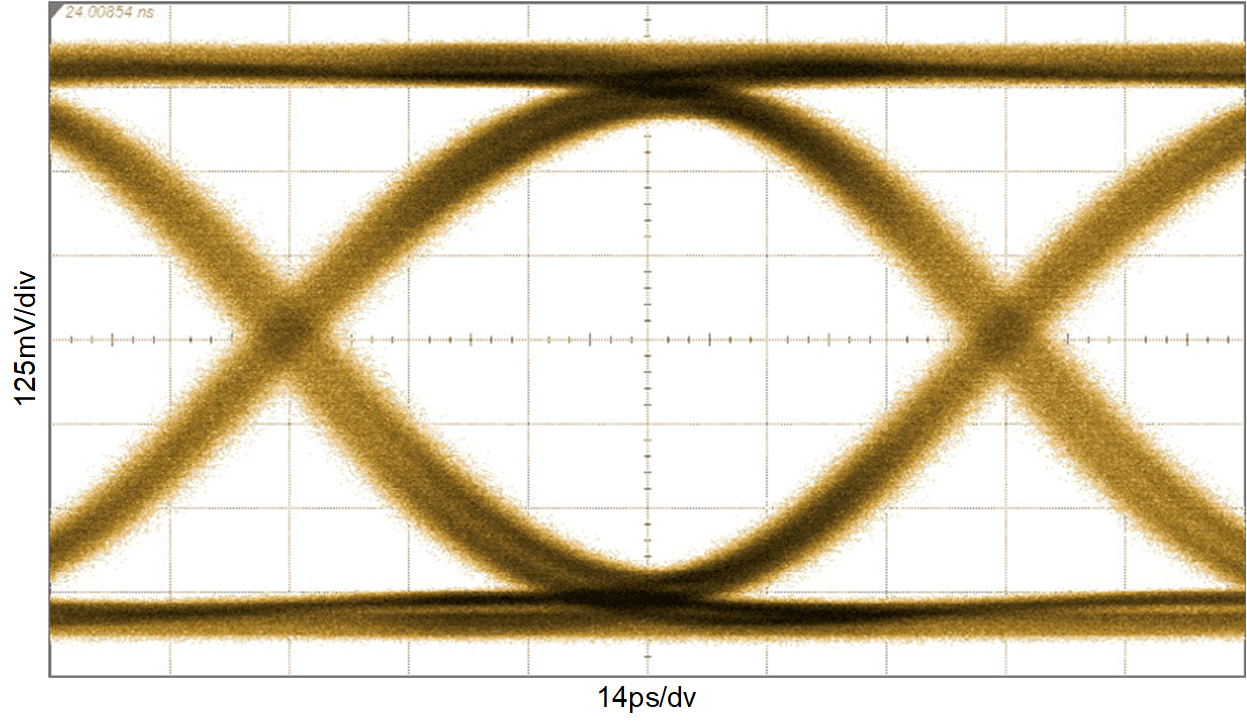
LMH1229 LMH1239 OUT0± at 11.88
           Gbps (12G-SDI), CC = 100m Belden 1694A, Reclocked
VOD_DE = F, SDI_OUT_SEL = H, OUT_CTRL = F
Figure 7-7 OUT0± at 11.88 Gbps (12G-SDI), CC = 100m Belden 1694A, Reclocked
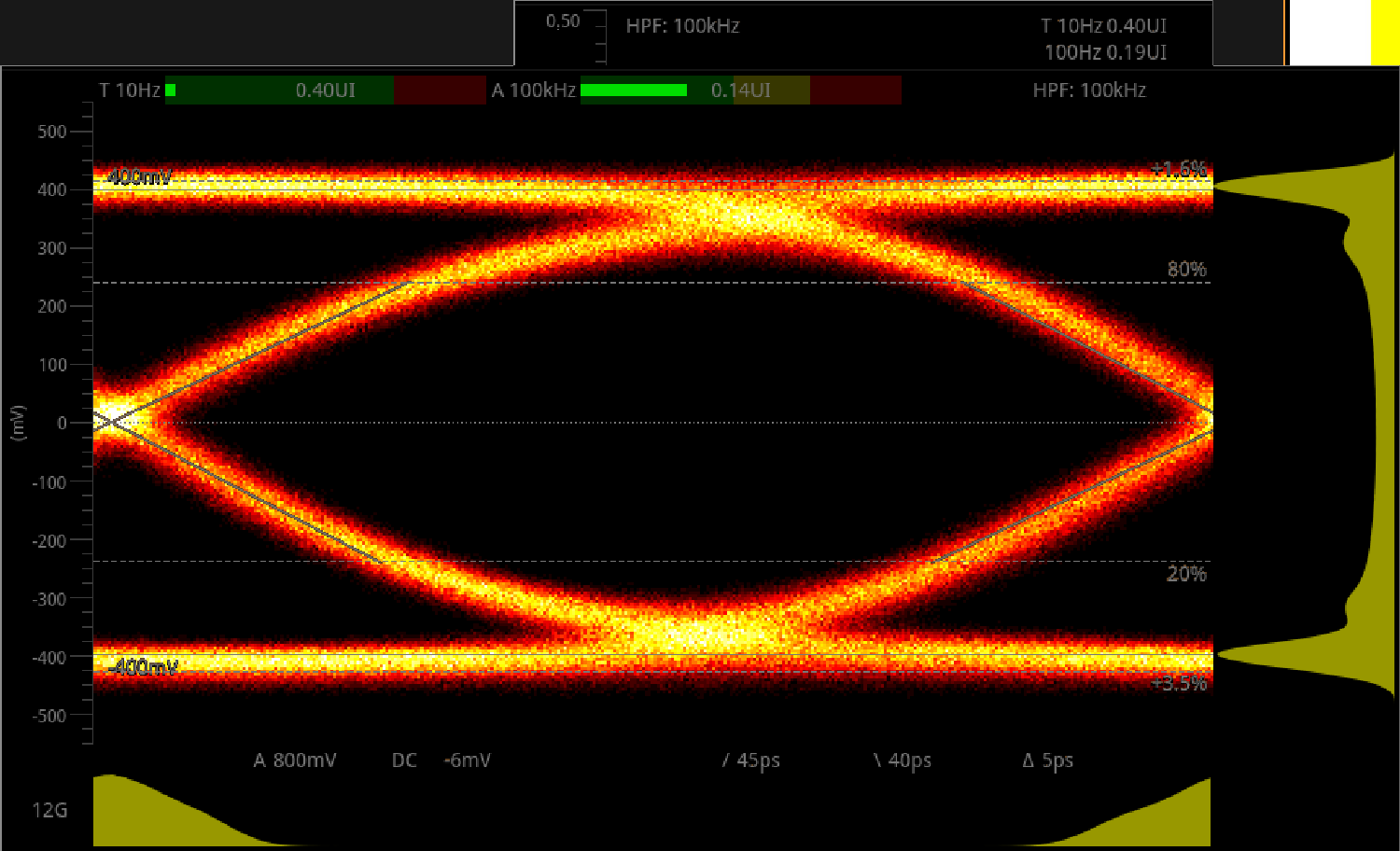
LMH1229 LMH1239 SDI_OUT+ at
            11.88Gbps (12G-SDI), CC = 90m Belden 1694A, Reclocked
VOD_DE = F, SDI_OUT_SEL = L, OUT_CTRL = F
Figure 7-9 SDI_OUT+ at 11.88Gbps (12G-SDI), CC = 90m Belden 1694A, Reclocked
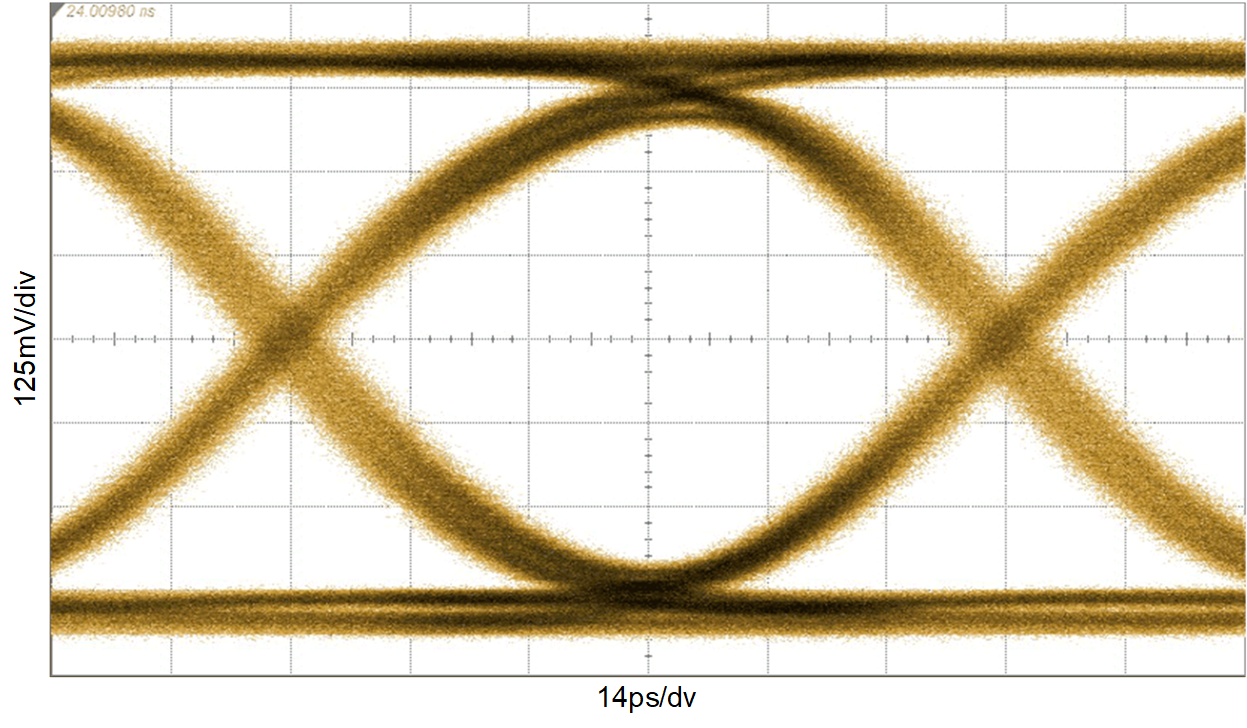
LMH1229 LMH1239 OUT1± at 11.88
           Gbps (12G-SDI), CC = 100m Belden 1694A, Reclocked
VOD_DE = F, SDI_OUT_SEL = H, OUT_CTRL = F
Figure 7-8 OUT1± at 11.88 Gbps (12G-SDI), CC = 100m Belden 1694A, Reclocked
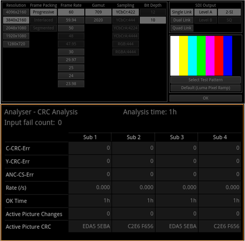
LMH1229 LMH1239 OUT0± BER at
            11.88Gbps (12G-SDI), CC = 100m Belden 1694A, Reclocked
VOD_DE = F, SDI_OUT_SEL = H, OUT_CTRL = F
Figure 7-10 OUT0± BER at 11.88Gbps (12G-SDI), CC = 100m Belden 1694A, Reclocked