JAJSNR7E May   2008  – July 2024 LMH6518

PRODUCTION DATA  

  1.   1
  2. 特長
  3. アプリケーション
  4. 概要
  5. Pin Configuration and Functions
  6. Specifications
    1. 5.1 Absolute Maximum Ratings
    2. 5.2 ESD Ratings
    3. 5.3 Recommended Operating Conditions
    4. 5.4 Thermal Information
    5. 5.5 Electrical Characteristics
    6. 5.6 Timing Requirements
    7. 5.7 Typical Characteristics
  7. Detailed Description
    1. 6.1 Overview
    2. 6.2 Functional Block Diagram
    3. 6.3 Feature Description
      1. 6.3.1 Input Preamplifier
        1. 6.3.1.1 Primary Output Amplifier
        2. 6.3.1.2 Auxiliary Amplifier
      2. 6.3.2 Overvoltage Clamp
      3. 6.3.3 Attenuator
      4. 6.3.4 Digital Control Block
    4. 6.4 Device Functional Modes
      1. 6.4.1 Primary Amplifier
      2. 6.4.2 Auxiliary Output
    5. 6.5 Programming
      1. 6.5.1 Logic Functions
  8. Application and Implementation
    1. 7.1 Application Information
    2. 7.2 Typical Application
      1. 7.2.1 Oscilloscope Front End
        1. 7.2.1.1 Design Requirements
        2. 7.2.1.2 Detailed Design Procedure
          1. 7.2.1.2.1 Settings and ADC SPI Code (ECM)
          2. 7.2.1.2.2 Input and Output Considerations
            1. 7.2.1.2.2.1 Output Swing, Clamping, and Operation Beyond Full Scale
          3. 7.2.1.2.3 Oscilloscope Trigger Applications
        3. 7.2.1.3 Application Curves
      2. 7.2.2 JFET LNA Implementation
        1. 7.2.2.1 Design Requirements
        2. 7.2.2.2 Detailed Design Procedure
          1. 7.2.2.2.1 Attenuator Design
        3. 7.2.2.3 Application Curve
    3. 7.3 Power Supply Recommendations
    4. 7.4 Layout
      1. 7.4.1 Layout Guidelines
      2. 7.4.2 Layout Example
  9. Device and Documentation Support
    1. 8.1 Device Support
      1. 8.1.1 サード・パーティ製品に関する免責事項
      2. 8.1.2 Device Nomenclature
    2. 8.2 Documentation Support
      1. 8.2.1 Related Documentation
    3. 8.3 ドキュメントの更新通知を受け取る方法
    4. 8.4 サポート・リソース
    5. 8.5 Trademarks
    6. 8.6 静電気放電に関する注意事項
    7. 8.7 用語集
  10. Revision History
  11. 10Mechanical, Packaging, and Orderable Information

パッケージ・オプション

メカニカル・データ(パッケージ|ピン)
サーマルパッド・メカニカル・データ
発注情報
Attenuator Design

Figure 7-12 shows a front-end attenuator designed to work with Figure 7-11.
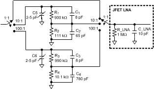
LMH6518 Front-End Attenuator for JFET LNA
                    ImplementationFigure 7-12 Front-End Attenuator for JFET LNA Implementation

R_LNA and C_LNA are the input impedance components of the JFET LNA. The 10:1 and 100:1 attenuators bottom resistors (R2 and R4) are adjusted higher to compensate for the LNA 1-MΩ input impedance, compared to the case where a high-input-impedance LNA is used. The two switches used on the input and output of the attenuator block are low-capacitance, high-isolation switches to reduce any speed or crosstalk impact. Capacitors C1 to C4 provide the proper frequency response (and step response) by creating zeros that flatten the response for wide-band operation. For the 10:1 attenuator, R1C1 = R2C2. The same applies to the 100:1 attenuator. The shunt capacitors, C1 to C4, have a important other benefit in that these capacitors roll off the resistor thermal noise at a low frequency (low-pass response, −3‑dB down at approximately 20‑kHz), thereby eliminating any significant noise contribution from the attenuation resistors. Otherwise, the channel noise is dominated by the attenuator resistor thermal noise. Adjust trimmer capacitors C5 and C6 to match the input capacitance regardless of attenuator used.