JAJSNR7E May 2008 – July 2024 LMH6518
PRODUCTION DATA
- 1
- 1 特長
- 2 アプリケーション
- 3 概要
- 4 Pin Configuration and Functions
- 5 Specifications
- 6 Detailed Description
- 7 Application and Implementation
- 8 Device and Documentation Support
- 9 Revision History
- 10Mechanical, Packaging, and Orderable Information
パッケージ・オプション
メカニカル・データ(パッケージ|ピン)
- RGH|16
サーマルパッド・メカニカル・データ
- RGH|16
発注情報
7.2.1.2.2 Input and Output Considerations
The LMH6518 ideal input and output conditions, considered individually, are listed in Table 7-2.
| IMPEDANCE FROM EACH INPUT TO GROUND (Ω) | COMMON MODE INPUT (V) | DIFFERENTIAL INPUT (VPP) | LOAD IMPEDANCE (Ω) | DIFFERENTIAL OUTPUT (V) | COMMON MODE OUTPUT (V) |
|---|---|---|---|---|---|
| ≤50 | 1.5 to 3.1 | < 0.8 | 100 (differential)
and 50 (single-ended) |
< 0.77 | 0.95 to 1.45 |
In addition to the individual conditions listed in Table 7-2, the input and output terminal conditions must match differentially (that is, +IN to −IN and +OUT to −OUT), as well, for best performance.
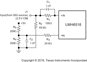
The input is differential but is driven single-ended as long as the conditions of Table 7-2 are met, and there is good matching between the driven and undriven inputs from DC to the highest frequency of interest. If not, there is a settling time impact among other possible performance degradations. The data-sheet specifications are with single-ended input, unless specified. Figure 7-4 is the recommended bench-test schematic to drive one input and to bias the other input with good matching in mind.
 Figure 7-4 Recommended Single-Ended Bench-Test Input Drive from 50-Ω Source
With Figure 7-4, each LMH6518 input sees 25-Ω to ground at higher frequencies when the capacitors look like shorts. This impedance increases to 125-Ω at DC for both inputs, thereby preserving the required matching at any frequency. This configuration, using properly selected R’s and C’s, allows four times less biasing power dissipation than when undriven inputs are biased with an effective 25-Ω from the LMH6518 input to ground.
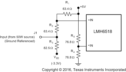
Driving the LMH6518 input from a ground-referenced, 50-Ω source is possible by providing level shift circuitry on the driven input. Figure 7-5 shows a circuit where half the input signal reaches the LMH6518 input, while the negative supply voltage (VEE) prevents biasing current on the 50-Ω source at J1 while providing 50-Ω termination to the source. The driven input (+IN) is biased to 2.5-V (VCC/2) in Figure 7-5.
 Figure 7-5 LMH6518 Driven by a Ground-Referenced
Source
Figure 7-5 LMH6518 Driven by a Ground-Referenced
SourceIn Figure 7-5, the equivalent impedance from each LMH6518 input to ground is around 38-Ω. The power consumption of this configuration is approximately 0.5 W (in R1 – R5) which is higher than that of Figure 7-4 because of additional power dissipated to perform the level shifting. Additional 50-Ω attenuators is placed between J1 and R2/R3 junction in Figure 7-5 to accommodate higher input voltages.
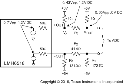
Shifting the LMH6518 output common mode level is also possible by using a level shift approach similar to that of Figure 7-5. The circuit in Figure 7-6 shows an implementation where the LMH6518 nominal 1.2-V CM output, set by a 1.2-V on VCM input from the GSPS ADC, is shifted lower for proper interface to different ADCs (which require VCM = 0-V and have high input impedance).
 Figure 7-6 Output CM Shift Scheme
In Figure 7-6, Vx is kept at 1.2-V by proper selection of external resistor values, so that the LMH6518 outputs are not CM-loaded. As was the case with input level shifting, this output-level shifting also consumes additional power (0.58 W).