JAJSNR7E May 2008 – July 2024 LMH6518
PRODUCTION DATA
- 1
- 1 特長
- 2 アプリケーション
- 3 概要
- 4 Pin Configuration and Functions
- 5 Specifications
- 6 Detailed Description
- 7 Application and Implementation
- 8 Device and Documentation Support
- 9 Revision History
- 10Mechanical, Packaging, and Orderable Information
パッケージ・オプション
メカニカル・データ(パッケージ|ピン)
- RGH|16
サーマルパッド・メカニカル・データ
- RGH|16
発注情報
6.5.1 Logic Functions
The following LMH6518 functions are controlled using the SPI-compatible bus:
- Filters (20 MHz, 100 MHz, 200 MHz, 350 MHz, 650 MHz, 750 MHz, or full bandwidth)
- Power mode (full power or auxiliary high impedance, Hi-Z)
- Preamp (HG or LG)
- Attenuation ladder (0 dB to 20 dB, 10 states)
- LMH6518 state write or read back
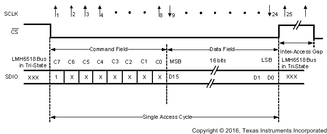
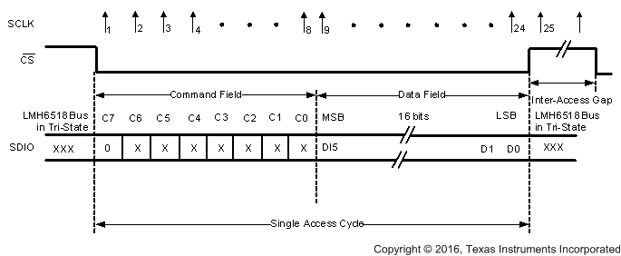
The SPI bus uses 3.3-V logic. SDIO is the serial digital input-output that writes to or reads back from the LMH6518. SCLK is the bus clock with chip-select function controlled by CS.
 Figure 6-1 Serial Interface Protocol, Read Operation
 Figure 6-2 Serial Interface Protocol, Write Operation
 Figure 6-3 Read Timing
 Figure 6-4 Write Timing
| FILTER | PREAMP | LADDER ATTENUATION | |||||||||||||
|---|---|---|---|---|---|---|---|---|---|---|---|---|---|---|---|
| D15 (MSB) |
D14 | D13 | D12 | D11 | D10 | D9 | D8 | D7 | D6 | D5 | D4 | D3 | D2 | D1 | D0 (LSB) |
| X | 0 | 0 | 0 | 0 | 0 = Full power 1 = Aux Hi-Z |
0 | See Table 6-3 | 0 | 0 = LG 1 = HG |
See Table 6-4 | |||||
Bits D5, D9, and D11 to D14 must be 0. Otherwise, device operation is undefined and specifications are not valid.
| FILTER | PREAMP | LADDER ATTENUATION | |||||||||||||
|---|---|---|---|---|---|---|---|---|---|---|---|---|---|---|---|
| D15 (MSB) |
D14 | D13 | D12 | D11 | D10 | D9 | D8 | D7 | D6 | D5 | D4 | D3 | D2 | D1 | D0 (LSB) |
| 0 | 0 | 0 | 0 | 0 | 0 | 0 | 0 | 0 | 0 | 0 | 0 | 1 | 0 | 1 | 0 |
| FILTER | BANDWIDTH (MHz) | ||
|---|---|---|---|
| D8 | D7 | D6 | |
| 0 | 0 | 0 | Full |
| 0 | 0 | 1 | 20 |
| 0 | 1 | 0 | 100 |
| 0 | 1 | 1 | 200 |
| 1 | 0 | 0 | 350 |
| 1 | 0 | 1 | 650 |
| 1 | 1 | 0 | 750 |
| 1 | 1 | 1 | Unallowed |
All filters are low-pass, single pole roll-off and operate on both main and auxiliary outputs. These filters are intended as signal path bandwidth and noise limiting.
| LADDER ATTENUATION | BANDWIDTH (dB) | |||
|---|---|---|---|---|
| D3 | D2 | D1 | D0 | |
| 0 | 0 | 0 | 0 | 0 |
| 0 | 0 | 0 | 1 | −2 |
| 0 | 0 | 1 | 0 | −4 |
| 0 | 0 | 1 | 1 | −6 |
| 0 | 1 | 0 | 0 | −8 |
| 0 | 1 | 0 | 1 | −10 |
| 0 | 1 | 1 | 0 | −12 |
| 0 | 1 | 1 | 1 | −14 |
| 1 | 0 | 0 | 0 | −16 |
| 1 | 0 | 0 | 1 | −18 |
| 1 | 0 | 1 | 0 | −20 |
| 1 | 0 | 1 | 1 | Unallowed |
| 1 | 1 | 0 | 0 | Unallowed |
| 1 | 1 | 0 | 1 | Unallowed |
| 1 | 1 | 1 | 0 | Unallowed |
| 1 | 1 | 1 | 1 | Unallowed |
An unallowed SPI state can result in undefined operation where device behavior is not valid.