JAJSNR7E May 2008 – July 2024 LMH6518
PRODUCTION DATA
- 1
- 1 特長
- 2 アプリケーション
- 3 概要
- 4 Pin Configuration and Functions
- 5 Specifications
- 6 Detailed Description
- 7 Application and Implementation
- 8 Device and Documentation Support
- 9 Revision History
- 10Mechanical, Packaging, and Orderable Information
パッケージ・オプション
メカニカル・データ(パッケージ|ピン)
- RGH|16
サーマルパッド・メカニカル・データ
- RGH|16
発注情報
7.2.1.2.2.1 Output Swing, Clamping, and Operation Beyond Full Scale
One of the major concerns when interfacing to low-voltage ADCs (such as the GSPS ADC that the LMH6518 is intended to drive) is to ensure that the ADC input is not violated with excessive drive. For this reason, plus the important requirement that an oscilloscope recovers quickly and gracefully from an overdrive condition, the LMH6518 is fitted with three overvoltage clamps: one at the preamp output, and one each at the main and auxiliary outputs. The preamp clamp is responsible for preventing the preamp from saturation (to minimize recovery time) with large ladder attenuation when preamp output swing is highest. Alternatively, the output clamps perform this function when ladder attenuation is lower. Therefore, the output amplifier is closer to saturation and prolonged recovery (if not properly clamped). The combination of these clamps results in Figure 5-50, Figure 5-51, Figure 5-52, and Figure 7-9. With these four graphs, observe where output limiting starts due to the clamp action. LMH6518 owes the fast recovery time (< 5 ns) from 50% overdrive to these clamps.
Figure 5-50, Figure 5-51, Figure 5-52, and Figure 7-9 in Section 5.7 are used to determine the LMH6518 linear swing beyond full scale. This information sets the overdrive limit for both oscilloscope waveform capture and signal triggering. The preamp clamp is set tighter than the output clamp, evidenced by lower output swing with 20-dB ladder attenuation than with 0 dB. With high ladder attenuation (20 dB) defining the limit, the graphs show that the +OUT and −OUT difference of 0.4-V is well inside the clamp range, thereby providing 0.8 VPP of unhindered output swing. This corresponds to an overdrive capability of approximately ±7% beyond full scale.
From Figure 7-1, the signal path consists of the input impedance switch, the attenuator switch, low-noise amplifier (LNA, JFET amplifier) to drive the LMH6518 input (+IN), and the DAC to provide offset adjust. The LNA must have the following characteristics:
- Set the U1 common-mode level to VCC / 2 (approximately 2.5 V)
- Low drift (1-mV shift at LNA output can translate into 88-mV shift at the LMH6518 output at maximum gain, or approximately 13% of FS)
- Low output impedance (≤ 50 Ω) to drive U1 for good settling behavior
- Low noise (< 0.98 nV/√Hz) to reduce the impact on the LMH6518 noise figure. Be aware that Figure 7-1 does not show the necessary capacitors across the resistors in the front-end attenuators (see Figure 7-12). These capacitors provide frequency response compensation and limit the noise contribution from the resistors so that the resistors do not impact the signal path noise. For more information about front-end attenuator design, including frequency compensation, see Section 8.2.1 for additional resources.
- Gain of 1 V/V (or close to 1 V/V)
- Excellent frequency response flatness from dc to > 500 MHz to 800 MHz to not impact the time domain performance
The undriven input (−IN) is biased to VCC / 2 using a voltage driver. The impedance driving the LMH6518 −IN pin must be closely matched to the LNA output impedance for good settling-time performance.
Section 7.2.2 shows one possible implementation of the LNA buffer along with performance data.
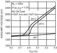
When the LMH6518 auxiliary output is not used, this output can be disabled using the SPI (see Section 6.5.1 for the SPI register map). Section 5.5 shows that by disabling this output, device power dissipation decreases by the reduction in supply current of approximately 60 mA. Figure 7-7 shows that in the absence of heavy common loading, the auxiliary output is at a voltage close to 1.7 V (VCC = 5 V). With higher supply voltages, the auxiliary voltage also increases. Ensure that any circuitry tied to this output is capable of handling the 2.3 V possible under VCC worst-case condition of 5.5 V.
 Figure 7-7 Auxiliary Output Voltage as a Function of VCC