at input CM = 2.5-V, VCM =
1.2-V, VCM AUX = 1.2-V, single-ended input drive, VCC = 5-V,
VDD = 3.3-V,
RL = 100 Ω
differential (both main and auxiliary outputs), VOUT = 0.7 VPP
differential (both main and auxiliary outputs), main output specification (auxiliary
is labeled), full bandwidth setting, gain = 18.8-dB (preamp LG, 0-dB ladder
attenuation), and full power setting (with auxiliary output turned on) (unless
otherwise noted)
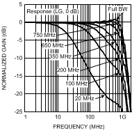
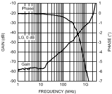
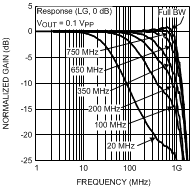
 Figure 5-1 Response (LG, 0-dB)
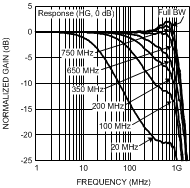
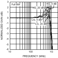
 Figure 5-3 Response (HG, 0-dB)
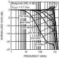
 Figure 5-5 Small
Signal Response (HG, 0-dB)
 Figure 5-7 Phase
vs Gain
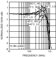
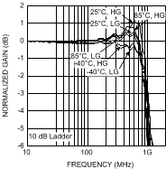
 Figure 5-9 Auxiliary Response Over Temperature
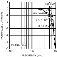
 Figure 5-11 Response vs Gain
 Figure 5-13 Response vs Gain
 Figure 5-15 Balance Error
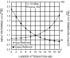
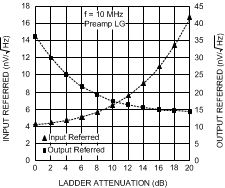
 Figure 5-17 Noise
vs Ladder Attenuation
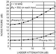
 Figure 5-19 Noise
Figure vs Gain
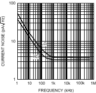
 Figure 5-21 Input
Current Noise vs Frequency
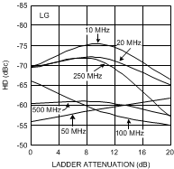
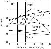
 Figure 5-23 HD3
vs Ladder Attenuation
 Figure 5-25 HD3
vs Ladder Attenuation
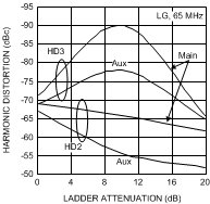
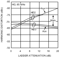
 Figure 5-27 Main
and Auxiliary Distortion Comparison
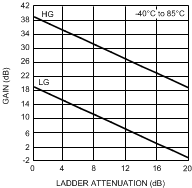
 Figure 5-29 Gain
vs Ladder Attenuation
 Figure 5-31 Auxiliary Gain Accuracy vs Ladder Attenuation
 Figure 5-33 AV_CM
 Figure 5-35 AV_CM
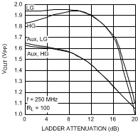
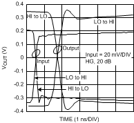
 Figure 5-37 Step
Response
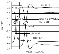
 Figure 5-39 Step
Response
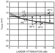
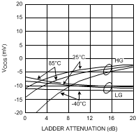
 Figure 5-41 Output Offset Voltage (Typical Unit 1)
 Figure 5-43 Output Offset Voltage (Typical Unit 3)
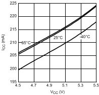
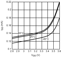
 Figure 5-45 Supply Current vs Supply Voltage
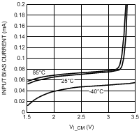
 Figure 5-47 Input
Bias Current vs Input CM
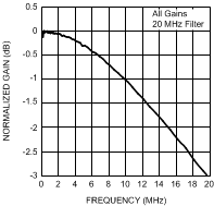
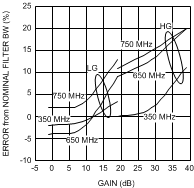
 Figure 5-49 Filter BW vs Gain
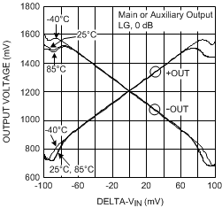
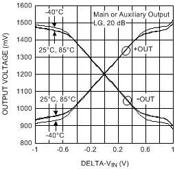
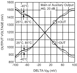
 Figure 5-51 Output vs Input
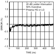
 Figure 5-53 Overdrive Recovery Time (Return to Zero)
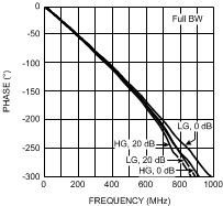
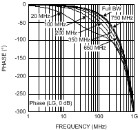
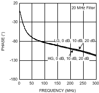
 Figure 5-2 Phase
(LG, 0-dB)
 Figure 5-4 Small
Signal Response (LG, 0-dB)
 Figure 5-6 Response vs Gain
 Figure 5-8 Response Over Temperature
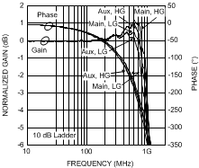
 Figure 5-10 Main
vs Auxiliary Response
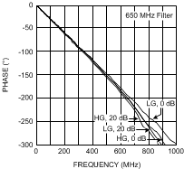
 Figure 5-12 Phase
vs Gain
 Figure 5-14 Phase
vs Gain
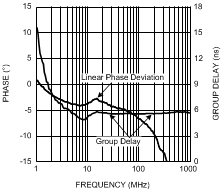
 Figure 5-16 Linear Phase Deviation and Group Delay
 Figure 5-18 Noise
vs Ladder Attenuation
 Figure 5-20 Input
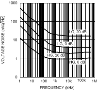
Voltage Noise vs Frequency
 Figure 5-22 HD2
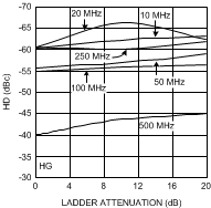
vs Ladder Attenuation
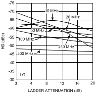
 Figure 5-24 HD2
vs Ladder Attenuation
 Figure 5-26 Main
and Auxiliary Distortion Comparison
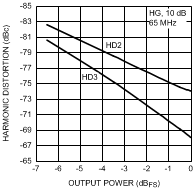
 Figure 5-28 Distortion vs Output Power
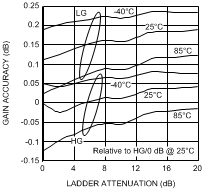
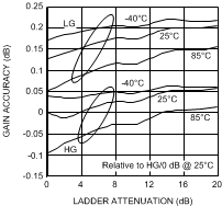
 Figure 5-30 Gain
Accuracy vs Ladder Attenuation
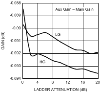
 Figure 5-32 Gain
Matching vs Ladder Attenuation
 Figure 5-34 AV_CM
 Figure 5-36 –1-dB
Compression vs Ladder Attenuation
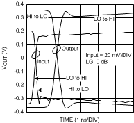
 Figure 5-38 Step
Response
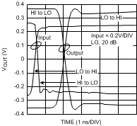
 Figure 5-40 Step
Response
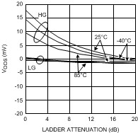
 Figure 5-42 Output Offset Voltage (Typical Unit 2)
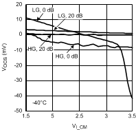
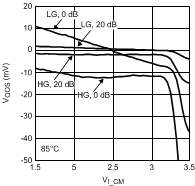
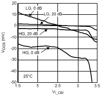
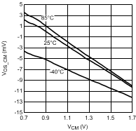
 Figure 5-44 VOS_CM vs VCM
 Figure 5-46 Supply Current vs Supply Voltage
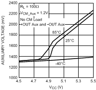
 Figure 5-48 Auxiliary Output Voltage (Hi-Z Mode)
 Figure 5-50 Output vs Input
 Figure 5-52 Output vs Input
