JAJSG10G June 2005 – August 2018 LMH6572
PRODUCTION DATA.
7.2.4 Expanding the Multiplexer
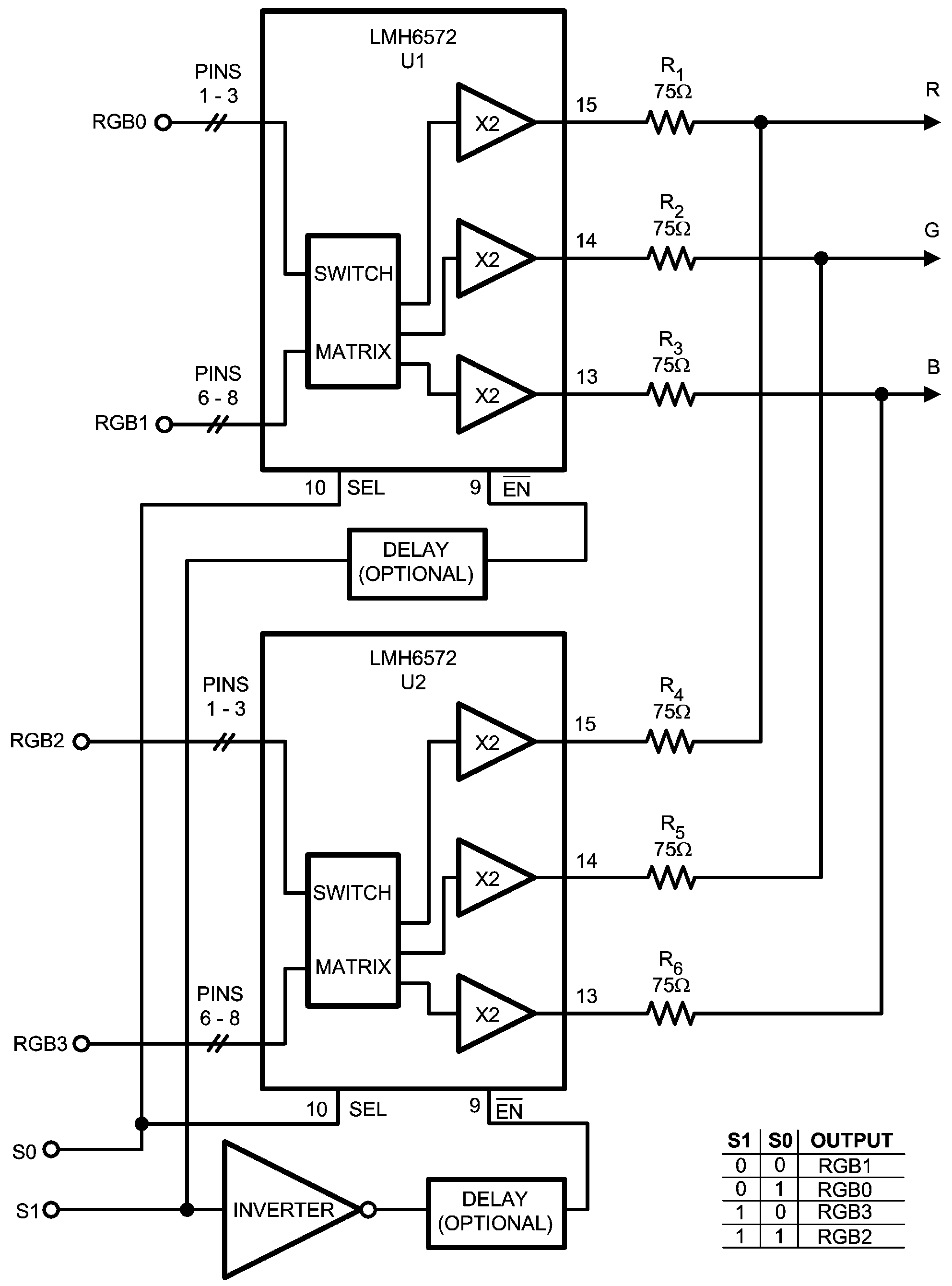
It is possible to build higher density multiplexers by paralleling several LMH6572s. Figure 20 shows a 4:1 RGB MUX using two LMH6572s:
 Figure 20. RGB MUX Using Two LMH6572's
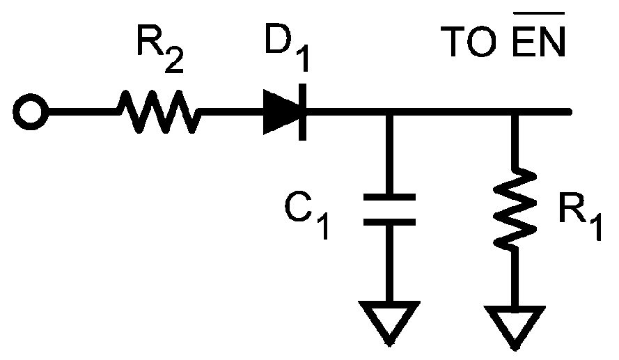
 If it is important in the end application to make sure that no two inputs are presented to the output at the same time, an optional delay block can be added prior to the ENABLE(EN) pin of each device, as shown. Figure 21 shows one possible approach to this delay circuit. The delay circuit shown will delay ENABLE’s H to L transitions (R1 and C1 decay) but will not delay its L to H transition.
 Figure 21. Delay Circuit Implementation
 R2 should be kept small compared to R1 in order to not reduce the ENABLE voltage and to produce little or no delay to the ENABLE L to H transition.
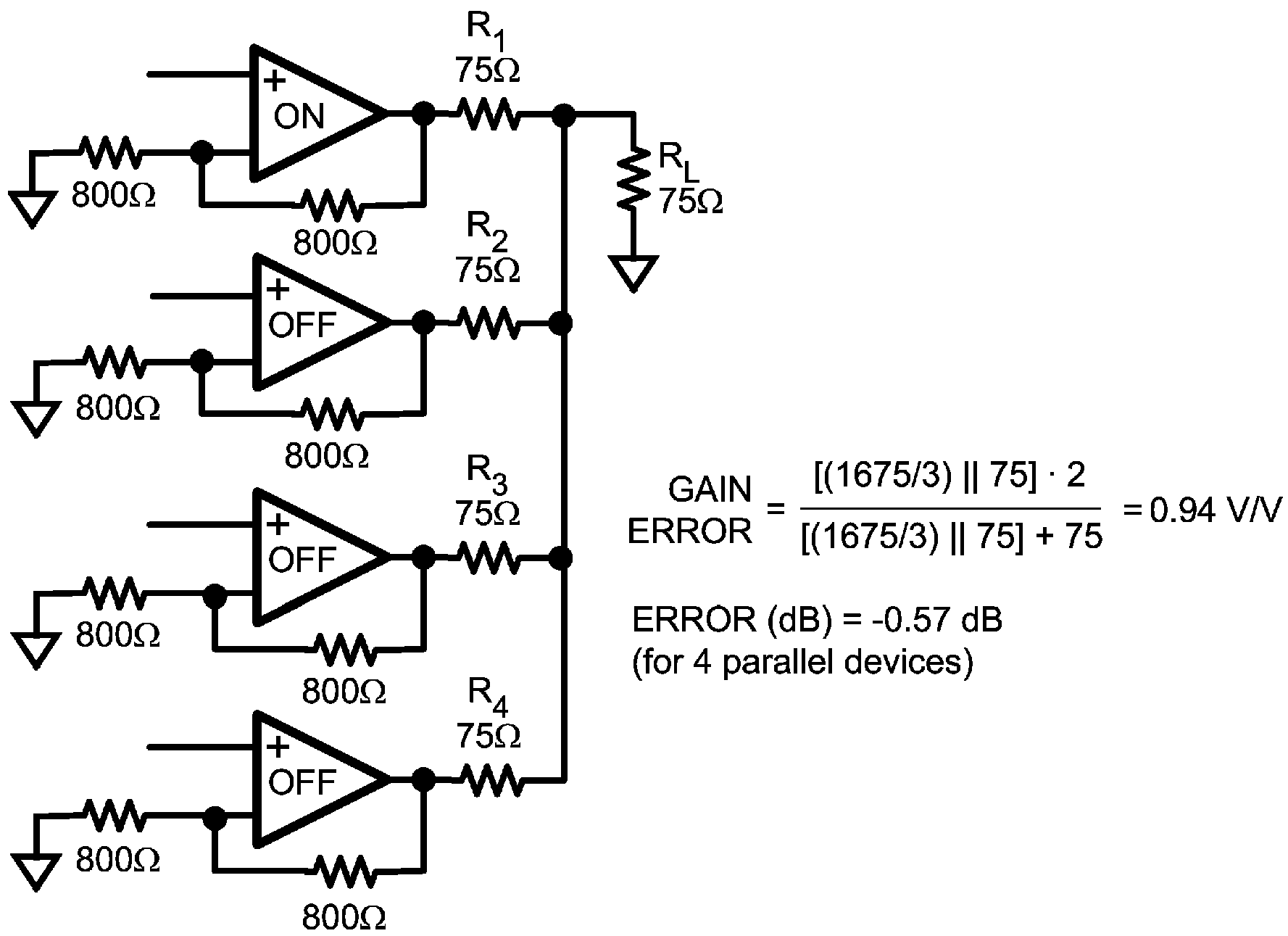
With the ENABLE pin putting the output stage into a high impedance state, several LMH6572’s can be tied together to form a larger input MUX. However, there is a slight loading effect on the active output caused by the off-channel feedback and gain set resistors, as shown in Figure 21. Figure 22 is assuming there are four LMH6572 devices tied together to form a triple 8:1 MUX. With the internal resistors valued at approximately 800Ω, the gain error is about -0.57 dB, or about −6%.
 Figure 22. Multiplexer Input Expansion by Combining Outputs
 An alternate approach would be to tie the outputs directly together and let all devices share a common back termination resistor in order to alleviate the gain error issue above.
The drawback in this case is the increased capacitive load presented to the output of each LMH6572 due to the offstate capacitance of the LMH6572.