JAJSDA8 June 2017 LMH6702-MIL
PRODUCTION DATA.
7 Detailed Description
7.1 Overview
The LMH6702-MIL has been optimized for exceptionally low harmonic distortion while driving very demanding resistive or capacitive loads. Generally, when used as the input amplifier to very high speed flash ADCs, the distortions introduced by the converter will dominate over the low LMH6702-MIL distortions shown in Typical Characteristics.
7.2 Feature Description
7.2.1 Harmonic Distortion
The capacitor CSS, shown across the supplies in Figure 24 and Figure 25, is critical to achieving the lowest 2nd harmonic distortion. For absolute minimum distortion levels, it is also advisable to keep the supply decoupling currents (ground connections to CPOS, and CNEG in Figure 24 and Figure 25) separate from the ground connections to sensitive input circuitry (such as RG, RT, and RIN ground connections). Splitting the ground plane in this fashion and separately routing the high frequency current spikes on the decoupling caps back to the power supply (similar to Star Connection layout technique) ensures minimum coupling back to the input circuitry and results in best harmonic distortion response (especially 2nd order distortion).
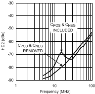
If this layout technique has not been observed on a particular application board, designer may actually find that supply decoupling caps could adversely affect HD2 performance by increasing the coupling phenomenon already mentioned. Figure 22 shows actual HD2 data on a board where the ground plane is shared between the supply decoupling capacitors and the rest of the circuit. Once these capacitors are removed, the HD2 distortion levels reduce significantly, especially between 10 MHz to 20 MHz, as shown in Figure 22:
 Figure 22. Decoupling Current Adverse Effect on a Board with Shared Ground Plane
At these extremely low distortion levels, the high frequency behavior of decoupling capacitors themselves could be significant. In general, lower value decoupling caps tend to have higher resonance frequencies making them more effective for higher frequency regions. A particular application board which has been laid out correctly with ground returns split to minimize coupling, would benefit the most by having low value and higher value capacitors paralleled to take advantage of the effective bandwidth of each and extend low distortion frequency range.
Another important variable in getting the highest fidelity signal from the LMH6702-MIL is the package itself. As already noted, coupling between high frequency current transients on supply lines and the device input can lead to excess harmonic distortion. An important source of this coupling is in fact through the device bonding wires. A smaller package, in general, will have shorter bonding wires and therefore lower coupling. This is true in the case of the SOT-23 compared to the SOIC package where a marked improvement in HD can be measured in the SOT-23 package. Figure 23 shows the HD comparing SOT-23 to SOIC package:
 Figure 23. SOIC and SOT-23 Packages Distortion Terms Compared
The LMH6702-MIL data sheet shows both SOT-23 and SOIC data in Electrical Characteristics to aid in selecting the right package. Typical Characteristics shows SOIC package plots only.
7.3 Device Functional Modes
7.3.1 2-Tone 3rd Order Intermodulation
Figure 10 shows a relatively constant difference between the test power level and the spurious level with the difference depending on frequency. The LMH6702-MIL does not show an intercept type performance, (where the relative spurious levels change at a 2X rate versus the test tone powers), due to an internal full power bandwidth enhancement circuit that boosts the performance as the output swing increases while dissipating negligible quiescent power under low output power conditions. This feature enhances the distortion performance and full power bandwidth to match that of much higher quiescent supply current parts.
7.3.2 DC Accuracy and Noise
The example in Equation 1 shows the output offset computation equation for the non-inverting configuration using the typical bias current and offset specifications for AV = 2:
Output Offset:
where
- RIN is the equivalent input impedance on the non-inverting input.
Example computation for AV = +2, RF = 237Ω, RIN = 25Ω:
A good design, however, should include a worst case calculation using min/max numbers in the data sheet tables, in order to ensure worst case operation.
Further improvement in the output offset voltage and drift is possible using the composite amplifiers described in Application Note OA--07, Current Feedback Op Amp Applications Circuit Guide (SNOA365). The two input bias currents are physically unrelated in both magnitude and polarity for the current feedback topology. It is not possible, therefore, to cancel their effects by matching the source impedance for the two inputs (as is commonly done for matched input bias current devices).
The total output noise is computed in a similar fashion to the output offset voltage. Using the input noise voltage and the two input noise currents, the output noise is developed through the same gain equations for each term but combined as the square root of the sum of squared contributing elements. See Application Note OA-12, Noise Analysis for Comlinear Amplifiers (SNOA375) for a full discussion of noise calculations for current feedback amplifiers.