JAJSA84E February 2005 – May 2016 LMH6703
PRODUCTION DATA.
- 1 特長
- 2 アプリケーション
- 3 概要
- 4 改訂履歴
- 5 Pin Configuration and Functions
- 6 Specifications
- 7 Typical Characteristics
- 8 Detailed Description
- 9 Application and Implementation
- 10Power Supply Recommendations
- 11Layout
- 12デバイスおよびドキュメントのサポート
- 13メカニカル、パッケージ、および注文情報
パッケージ・オプション
メカニカル・データ(パッケージ|ピン)
サーマルパッド・メカニカル・データ
発注情報
11 Layout
11.1 Layout Guidelines
Whenever questions about layout arise, use the evaluation board (see Table 1) as a guide. The LMH730216 is the evaluation board for SOT-23-6 samples and the LMH730227 is the evaluation board for SOIC samples.
To reduce parasitic capacitances, ground and power planes should be removed near the input and output pins. Components in the feedback path should be placed as close to the device as possible to minimize parasitic capacitance. For long signal paths controlled impedance lines should be used, along with impedance matching elements at both ends.
Bypass capacitors should be placed as close to the device as possible. Bypass capacitors from each voltage rail to ground are applied in pairs. The larger electrolytic bypass capacitors can be located further from the device, the smaller ceramic bypass capacitors should be placed as close to the device as possible. In Figure 29 and Figure 30, CSS is optional, but is recommended for best second order harmonic distortion.
Generally, a good high frequency layout will keep power supply and ground traces away from the inverting input and output pins. Parasitic capacitances on these nodes to ground will cause frequency response peaking and possible circuit oscillations. See Frequent Faux Pas in Applying Wideband Current Feedback Amplifiers, Application Note OA-15 (SNOA367). The evaluation board(s) is a good example of high frequency layout techniques as a reference.
General high-speed, signal-path layout suggestions include:
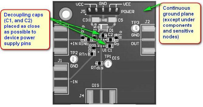
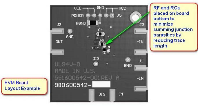
- Continuous ground planes are preferred for signal routing, as shown in Figure 33 and Figure 34, with matched impedance traces for longer runs. However, open up both ground and power planes around the capacitive sensitive input and output device pins.
- Use good, high-frequency decoupling capacitors (0.1 μF) on the ground plane at the device power pins as shown in Figure 33. Higher value capacitors (2.2 μF) are required, but may be placed further from the device power pins and shared among devices. For best high-frequency decoupling, consider X2Y supply-decoupling capacitors that offer a much higher self-resonance frequency over standard capacitors.
- When using differential signal routing over any appreciable distance, use microstrip layout techniques with matched impedance traces.
- The input summing junction is very sensitive to parasitic capacitance. Connect any Rf, and Rg elements into the summing junction with minimal trace length to the device pin side of the resistor, as shown in Figure 34. The other side of these elements can have more trace length if needed to the source or to ground.
Table 1. Evaluation Boards
| DEVICE | PACKAGE | EVALUATION BOARD PART NUMBER |
| LMH6703MF | SOT-23-6 | LMH730216 |
| LMH6703MA | SOIC | LMH730227 |
11.2 Layout Example
 Figure 33. Evaluation Board Layer 1
 Figure 34. Evaluation Board Layer 2