SNVSAL6A July 2016 – February 2017 LMP8480-Q1 , LMP8481-Q1
PRODUCTION DATA.
- 1 Features
- 2 Applications
- 3 Description
- 4 Revision History
- 5 Device Comparison Table
- 6 Pin Configuration and Functions
- 7 Specifications
-
8 Detailed Description
- 8.1 Overview
- 8.2 Functional Block Diagrams
- 8.3
Feature Description
- 8.3.1 Basic Connections
- 8.3.2 Selection of the Sense Resistor
- 8.3.3 Using PCB Traces as Sense Resistors
- 8.3.4 VREFA and VREFB Pins (LMP8481-Q1 Only)
- 8.3.5 Reference Input Voltage Limits (LMP8481-Q1 Only)
- 8.3.6 Low-Side Current Sensing
- 8.3.7 Input Series Resistance
- 8.3.8 Minimum Output Voltage
- 8.3.9 Swinging Output Below Ground
- 8.3.10 Maximum Output Voltage
- 8.4 Device Functional Modes
- 9 Application and Implementation
- 10Power Supply Recommendations
- 11Layout
- 12Device and Documentation Support
- 13Mechanical, Packaging, and Orderable Information
1 Features
- Qualified for Automotive Applications
- AEC-Q100 Qualified With the Following Results:
- Device Temperature Grade 1: –40°C to 125°C Ambient Operating Temperature
- Device HBM ESD Classification Level 2
- Device CDM ESD Classification Level C6
- Bidirectional or Unidirectional Sensing
- Common Mode Voltage Range: 4.0 V to 76 V
- Supply Voltage Range: 4.5 V to 76 V
- Fixed Gains: 20, 60, and 100 V/V
- Gain Accuracy: ±0.1%
- Offset: ±80 µV
- Bandwidth (–3 dB): 270 kHz
- Quiescent Current: < 100 µA
- Buffered High-Current Output: > 5 mA
- Input Bias Current: 7 µA
- PSRR (DC): 122 dB
- CMRR (DC): 124 dB
2 Applications
- Body Control Modules
- Powertrain
- Battery Management
- Inverters
3 Description
The automotive-qualified LMP8480-Q1 and LMP8481-Q1 devices are precision, high-side, current-sense amplifiers that amplify a small differential voltage developed across a current-sense resistor in the presence of high input common-mode voltages. These amplifiers are designed for bidirectional (LMP8481-Q1) or unidirectional (LMP8480-Q1) current applications and accept input signals with a common-mode voltage range from 4 V to 76 V with a bandwidth of 270 kHz. Because the operating power-supply range overlaps the input common-mode voltage range, the LMP848x-Q1 can be powered by the same voltage that is being monitored. This benefit eliminates the need for an intermediate supply voltage to be routed to the point of load where the current is being monitored, resulting in reduced component count and board space.
The LMP848x-Q1 family consists of fixed gains of 20, 60, and 100 for applications that demand high accuracy over temperature. The low-input offset voltage allows the use of smaller sense resistors without sacrificing system error. The LMP8480-Q1 and LMP8481-Q1 are pin-for-pin replacements for the MAX4080 and MAX4081 devices, offering improved offset voltage, wider reference adjust range, and higher output drive capabilities. The LMP8480-Q1 and LMP8481-Q1 are available in an 8-pin VSSOP package.
Device Information(1)
| PART NUMBER | PACKAGE | BODY SIZE (NOM) |
|---|---|---|
| LMP8480-Q1 | VSSOP (8) | 3.00 mm x 3.00 mm |
| LMP8481-Q1 | VSSOP (8) | 3.00 mm x 3.00 mm |
- For all available packages, see the orderable addendum at the end of the data sheet.
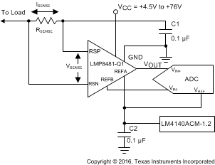
Typical Application Schematic
