SNVSAL6A July 2016 – February 2017 LMP8480-Q1 , LMP8481-Q1
PRODUCTION DATA.
- 1 Features
- 2 Applications
- 3 Description
- 4 Revision History
- 5 Device Comparison Table
- 6 Pin Configuration and Functions
- 7 Specifications
-
8 Detailed Description
- 8.1 Overview
- 8.2 Functional Block Diagrams
- 8.3
Feature Description
- 8.3.1 Basic Connections
- 8.3.2 Selection of the Sense Resistor
- 8.3.3 Using PCB Traces as Sense Resistors
- 8.3.4 VREFA and VREFB Pins (LMP8481-Q1 Only)
- 8.3.5 Reference Input Voltage Limits (LMP8481-Q1 Only)
- 8.3.6 Low-Side Current Sensing
- 8.3.7 Input Series Resistance
- 8.3.8 Minimum Output Voltage
- 8.3.9 Swinging Output Below Ground
- 8.3.10 Maximum Output Voltage
- 8.4 Device Functional Modes
- 9 Application and Implementation
- 10Power Supply Recommendations
- 11Layout
- 12Device and Documentation Support
- 13Mechanical, Packaging, and Orderable Information
11 Layout
11.1 Layout Guidelines
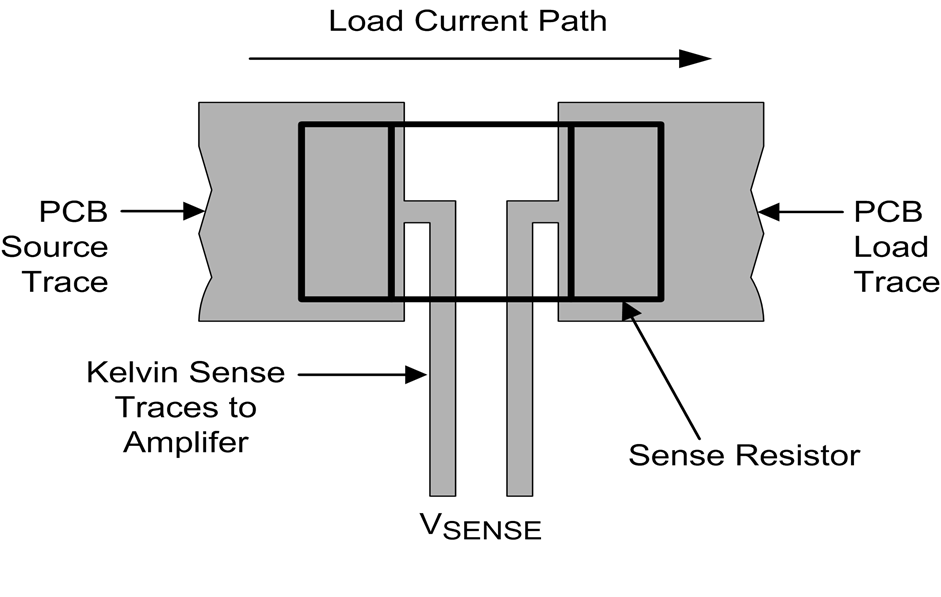
The traces leading to and from the sense resistor can be significant error sources. With small value sense resistors (< 100 mΩ), any trace resistance shared with the load current can cause significant errors.
The amplifier inputs must be directly connected to the sense resistor pads using Kelvin or 4-wire connection techniques. The traces must be one continuous piece of copper from the sense resistor pad to the amplifier input pin pad, and ideally on the same copper layer with minimal vias or connectors. These recommendations can be important around the sense resistor if any significant heat gradients are being generated.
To minimize noise pickup and thermal errors, the input traces must be treated as a differential signal pair and routed tightly together with a direct path to the input pins. The input traces must be run away from noise sources, such as digital lines, switching supplies or motor drive lines. Remember that these traces can contain high voltage, and must have the appropriate trace routing clearances.
Because the sense traces only carry the amplifier bias current (approximately 7 µA at room temperature), the connecting input traces can be thinner, signal level traces. Excessive resistance in the trace must also be avoided.
The paths of the traces must be identical, including connectors and vias, so that these errors are equal and cancel.
The sense resistor heats up when the load increases. When the resistor heats up, the resistance generally goes up, which causes a change in the readings. The sense resistor must have as much heatsinking as possible to remove this heat through the use of heatsinks or large copper areas coupled to the resistor pads. A reading drifting over time after turn-on can usually be traced back to sense resistor heating.
11.2 Layout Example
 Figure 32. Kelvin or 4–Wire Connection to the Sense Resistor