JAJSOI8H November   2009  – May 2022 LMP8645 , LMP8645HV

PRODUCTION DATA  

  1. 特長
  2. アプリケーション
  3. 概要
  4. Revision History
  5. Pin Configuration and Functions
  6. Specifications
    1. 6.1 Absolute Maximum Ratings
    2. 6.2 ESD Ratings
    3. 6.3 Recommended Operating Conditions
    4. 6.4 Thermal Information
    5. 6.5 2.7-V Electrical Characteristics
    6. 6.6 5-V Electrical Characteristics
    7. 6.7 12-V Electrical Characteristics
    8. 6.8 Typical Characteristics
  7. Detailed Description
    1. 7.1 Overview
      1. 7.1.1 Theory of Operation
    2. 7.2 Functional Block Diagram
    3. 7.3 Feature Description
      1. 7.3.1 Driving ADC
      2. 7.3.2 Applying Input Voltage With No Supply Voltage
    4. 7.4 Device Functional Modes
      1. 7.4.1 Selection of the Gain Resistor
      2. 7.4.2 Gain Range Limitations
        1. 7.4.2.1 Range 1: VCM is –2 V to 1.8 V
        2. 7.4.2.2 Range 2: VCM is 1.8 V to VS
        3. 7.4.2.3 Range 3: VCM is greater than VS
      3. 7.4.3 Selection of Sense Resistor
        1. 7.4.3.1 Resistor Power Rating and Thermal Issues
        2. 7.4.3.2 Using PCB Trace as a Sense Resistor
      4. 7.4.4 Sense Line Inputs
        1. 7.4.4.1 Effects of Series Resistance on Sense Lines
  8. Application and Implementation
    1. 8.1 Application Information
    2. 8.2 Typical Applications
      1. 8.2.1 Typical Current Monitor Application
        1. 8.2.1.1 Design Requirements
        2. 8.2.1.2 Detailed Design Procedure
        3. 8.2.1.3 Application Curves
      2. 8.2.2 High Brightness LED Driver
  9. Power Supply Recommendations
  10. 10Layout
    1. 10.1 Layout Guidelines
    2. 10.2 Layout Example
  11. 11Device and Documentation Support
    1. 11.1 Device Support
      1. 11.1.1 Development Support
    2. 11.2 Documentation Support
      1. 11.2.1 Related Documentation
    3. 11.3 Receiving Notification of Documentation Updates
    4. 11.4 サポート・リソース
    5. 11.5 Trademarks
    6. 11.6 Electrostatic Discharge Caution
    7. 11.7 Glossary
  12. 12Mechanical, Packaging, and Orderable Information

パッケージ・オプション

メカニカル・データ(パッケージ|ピン)
サーマルパッド・メカニカル・データ
発注情報

Application Curves

Figure 8-2 shows the resulting circuit voltages with the input load swept from 0 A to 1 A, with RGAIN= 13 kΩ for operation in Range 1 (preferring accuracy over all load operating conditions).

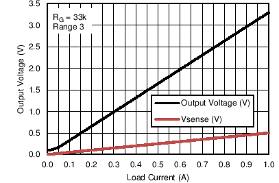
Also shown in Figure 8-3 is the resulting output voltage with RGAIN = 33 kΩ for operation in Range 3 (sacrificing low load supply accuracy while optimizing overall resolution at normal load operating conditions).
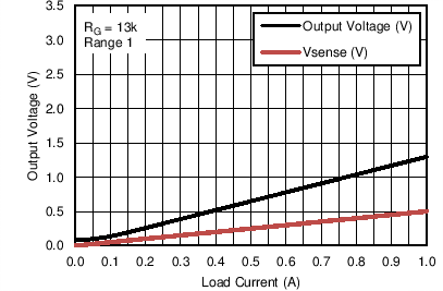
GUID-EFEF1954-A989-44AE-AACC-E8BB45C9FECA-low.pngFigure 8-2 Resulting Input and Output Voltages vs Load Current for Range 1
GUID-AC69A6A6-78ED-4B89-B11E-817A714DC6E0-low.pngFigure 8-3 Resulting Input and Output Voltages vs Load Current For Range 3