SNIS163B April   2012  – October 2015 LMP91002

PRODUCTION DATA.  

  1. Features
  2. Applications
  3. Description
  4. Revision History
  5. Pin Configuration and Functions
  6. Specifications
    1. 6.1 Absolute Maximum Ratings
    2. 6.2 ESD Ratings
    3. 6.3 Recommended Operating Conditions
    4. 6.4 Thermal Information
    5. 6.5 Electrical Characteristics
    6. 6.6 I2C Interface
    7. 6.7 Timing Characteristics
    8. 6.8 Typical Characteristics
  7. Detailed Description
    1. 7.1 Overview
    2. 7.2 Functional Block Diagram
    3. 7.3 Feature Description
      1. 7.3.1 Potentiostat Circuitry
      2. 7.3.2 Transimpedance Amplifier
      3. 7.3.3 Control Amplifier
      4. 7.3.4 Internal Zero
      5. 7.3.5 2-Lead Galvanic Cell in Potentiostat Configuration
    4. 7.4 Device Functional Modes
      1. 7.4.1 Timeout Feature
    5. 7.5 Programming
      1. 7.5.1 I2C Interface
      2. 7.5.2 Write and Read Operation
      3. 7.5.3 Connection of More Than One LMP91002 to the I2C Bus
    6. 7.6 Register Maps
      1. 7.6.1 STATUS Register (Offset = 00h)
      2. 7.6.2 LOCK Register (Offset = 01h)
      3. 7.6.3 TIACN Register (Offset = 10h)
      4. 7.6.4 REFCN Register (Offset = 11h)
      5. 7.6.5 MODECN Register (Offset = 12h)
  8. Application and Implementation
    1. 8.1 Application Information
      1. 8.1.1 Gas Sensor Interface
        1. 8.1.1.1 3-Lead Amperometric Cell In Potentiostat Configuration
      2. 8.1.2 Sensor Test Procedure
    2. 8.2 Typical Application
      1. 8.2.1 Design Requirements
      2. 8.2.2 Detailed Design Procedure
        1. 8.2.2.1 Smart Gas Sensor Analog Front End
        2. 8.2.2.2 Smart Gas Sensor AFES on I2C Bus
      3. 8.2.3 Application Curves
  9. Power Supply Recommendations
    1. 9.1 Power Consumption
  10. 10Layout
    1. 10.1 Layout Guidelines
    2. 10.2 Layout Example
  11. 11Device and Documentation Support
    1. 11.1 Community Resources
    2. 11.2 Trademarks
    3. 11.3 Electrostatic Discharge Caution
    4. 11.4 Glossary
  12. 12Mechanical, Packaging, and Orderable Information

パッケージ・オプション

メカニカル・データ(パッケージ|ピン)
サーマルパッド・メカニカル・データ
発注情報

5 Pin Configuration and Functions

NHL Package
14-Pin WSON
Top View
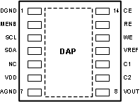
LMP91002 30182502.gif

Pin Functions(1)

PIN I/O DESCRIPTION
NO. NAME
1 DGND G Connect to ground
2 MENB D Module Enable. Active Low
3 SCL D I2C Clock
4 SDA D I2C Data
5 NC Do not connect. Not internally connected
6 VDD P Voltage supply
7 AGND GND Analog GND
8 VOUT A Analog voltage representing sensor output
9 C2 A Optional External component node 2 for TIA (filter capacitor or gain resistor)
10 C1 A Optional External component node 1 for TIA (filter capacitor or gain resistor)
11 VREF A External Reference voltage input
12 WE A Working Electrode of the sensor.
13 RE A Reference Electrode of the sensor.
14 CE A Counter Electrode of the sensor.
DAP GND Die attached pad. Connect to GND.
(1) A = analog, D = digital, P = power, G = GND