SNAS517E November 2011 – September 2015 LMP91050
PRODUCTION DATA.
- 1 Features
- 2 Applications
- 3 Description
- 4 Revision History
- 5 Description (continued)
- 6 Pin Configuration and Functions
- 7 Specifications
- 8 Detailed Description
- 9 Application and Implementation
- 10Power Supply Recommendations
- 11Layout
- 12Device and Documentation Support
- 13Mechanical, Packaging, and Orderable Information
9 Application and Implementation
NOTE
Information in the following applications sections is not part of the TI component specification, and TI does not warrant its accuracy or completeness. TI’s customers are responsible for determining suitability of components for their purposes. Customers should validate and test their design implementation to confirm system functionality.
9.1 Application Information
Figure 26 shows a typical NDIR sensing circuit with a bandpass filter with a high frequency cutoff of approximately 100 Hz. The lowpass filter at the output has a cutoff of approximately 110 Hz.
9.2 Typical Application
 Figure 26. Typical NDIR Sensing Application Circuit
9.2.1 Design Requirements
The design requirements for using the LMP91050 in an application basically include the following:
- Determine the characteristics of the thermopile and the appropriate gain and common mode voltage that will maximize the dynamic range of the sensor. Consult the manufacturer’s data sheet.
- Selecting an analog-to-digital converter that supports the needed resolution and update rate.
- Determining the bandwidth of the inter-stage low-pass filter to limit the noise imposed on the signal
- An SPI interface to a microcontroller or other logic device is required in order to configure the LMP91050.
9.2.2 Detailed Design Procedure
The basic design procedure is as follows:
- Select the appropriate inter-stage bandpass filter bandwidth. Note that the common mode voltage (CMOUT) is connected to both the thermopile and the bandpass filter, as shown in Figure 26.
- TI recommends that a lowpass filter be inserted between the OUT pin and the input to the ADC, to further reduce noise on the signal and prevent aliasing.
- Power supply bypassing as shown in figure 32 is recommended.
- Based on the thermopile characteristics, select the common-mode voltage and gain to be programmed into the LMP91050. CMOUT should be selected to center the expected dynamic range of the thermopile within the full scale range of the ADC to the best extent possible. The gain should be selected to maximize the signal range at the ADC input, but should allow some headroom below full scale to prevent clipping. The gain should also compensate, if possible, for any loss due to the filters in the signal path.
- The internal DAC can be programmed to further optimize the signal range on the OUT pin. See Offset Adjust for further information.
9.2.3 Application Curves
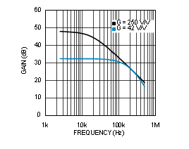
 Figure 27. PGA1 Small Signal Bandwidth
 Figure 29. Power Supply Rejection Ratio vs. Frequency
 Figure 31. DAC DC Sweep With VDD = 3.3 V
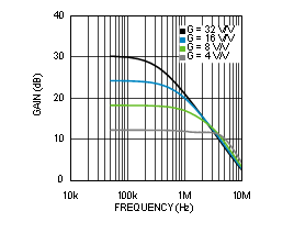
 Figure 28. PGA2 Small Signal Bandwidth
 Figure 30. Input-Referred Noise Density vs. Frequency
 Figure 32. DAC DC Sweep With VDD = 5 V