SNAS517E November 2011 – September 2015 LMP91050
PRODUCTION DATA.
- 1 Features
- 2 Applications
- 3 Description
- 4 Revision History
- 5 Description (continued)
- 6 Pin Configuration and Functions
- 7 Specifications
- 8 Detailed Description
- 9 Application and Implementation
- 10Power Supply Recommendations
- 11Layout
- 12Device and Documentation Support
- 13Mechanical, Packaging, and Orderable Information
7 Specifications
7.1 Absolute Maximum Ratings
over operating free-air temperature range (unless otherwise noted)(2)(1)(4)| MIN | MAX | UNIT | ||
|---|---|---|---|---|
| Supply Voltage (VDD) | –0.3 | 6 | V | |
| Voltage at Any Pin | –0.3 | VDD + 0.3 | V | |
| Input Current at Any Pin | 5 | mA | ||
| Junction Temperature(3) | 150 | °C | ||
| Storage Temperature, Tstg | –65 | 150 | °C | |
(1) If Military/Aerospace specified devices are required, please contact the Texas Instruments Sales Office/ Distributors for availability and specifications.
(2) Stresses beyond those listed under Absolute Maximum Ratings may cause permanent damage to the device. These are stress ratings only, which do not imply functional operation of the device at these or any other conditions beyond those indicated under Recommended Operating Conditions. Exposure to absolute-maximum-rated conditions for extended periods may affect device reliability.
(3) The maximum power dissipation is a function of TJ(MAX), θJA, and the ambient temperature, TA. The maximum allowable power dissipation at any ambient temperature is PDMAX = (TJ(MAX) - TA)/ θJA All numbers apply for packages soldered directly onto a PC board.
(4) For soldering specifications: see product folder at www.ti.com and SNOA549.
7.2 ESD Ratings
| VALUE | UNIT | |||
|---|---|---|---|---|
| V(ESD) | Electrostatic discharge | Human body model (HBM), per ANSI/ESDA/JEDEC JS-001(1) | ±2500 | V |
| Charged-device model (CDM), per JEDEC specification JESD22-C101(2) | ±1250 | |||
| Machine Model | ±250 | |||
(1) JEDEC document JEP155 states that 500-V HBM allows safe manufacturing with a standard ESD control process.
(2) JEDEC document JEP157 states that 250-V CDM allows safe manufacturing with a standard ESD control process.
7.3 Recommended Operating Conditions
over operating free-air temperature range (unless otherwise noted)(1)| MIN | MAX | UNIT | ||
|---|---|---|---|---|
| Supply Voltage | 2.7 | 5.5 | V | |
| Junction Temperature(2) | –40 | 105 | °C | |
(1) Stresses beyond those listed under Absolute Maximum Ratings may cause permanent damage to the device. These are stress ratings only, which do not imply functional operation of the device at these or any other conditions beyond those indicated under Recommended Operating Conditions. Exposure to absolute-maximum-rated conditions for extended periods may affect device reliability.
(2) The maximum power dissipation is a function of TJ(MAX), θJA, and the ambient temperature, TA. The maximum allowable power dissipation at any ambient temperature is PDMAX = (TJ(MAX) - TA)/ θJA All numbers apply for packages soldered directly onto a PC board.
7.4 Thermal Information
| THERMAL METRIC(1) | LMP91050 | UNIT | |
|---|---|---|---|
| DGS (VSSOP) | |||
| 10 PINS | |||
| RθJA | Junction-to-ambient thermal resistance | 176 | °C/W |
(1) For more information about traditional and new thermal metrics, see the Semiconductor and IC Package Thermal Metrics application report, SPRA953.
7.5 Electrical Characteristics
The following specifications apply for VDD = 3.3 V, VCM = 1.15 V, unless otherwise specified. All other limits apply to TA = TJ = +25°C.(1)| PARAMETER | TEST CONDITIONS | MIN(3) | TYP(2) | MAX(3) | UNIT | |
|---|---|---|---|---|---|---|
| POWER SUPPLY | ||||||
| VDD | Supply voltage | 2.7 | 3.3 | 5.5 | V | |
| IDD | Supply current | All analog block ON | 3.1 | 3.7 | 4.2 | mA |
| Power-down supply current | All analog block OFF | 45 | 85 | 121 | μA | |
| OFFSET CANCELLATION (OFFSET DAC) | ||||||
| Resolution | 256 | steps | ||||
| LSB | All gains | 33.8 | mV | |||
| DNL | -1 | 2 | LSB | |||
| Error | Output referred offset error, all gains | ±100 | mV | |||
| Offset adjust range | Output referred, all gains | 0.2 | VDD – 0.2 | V | ||
| DAC settling time | 480 | μs | ||||
| PROGRAMMABLE GAIN AMPLIFIER (PGA) 1ST STAGE, RL = 10 kΩ, CL = 15 pF | ||||||
| IBIAS | Bias current | 5 | pA | |||
| TA = –40°C to +85°C | 200 | |||||
| VINMAX _HGM |
Max input signal high-gain mode | Referenced to CMOUT voltage, it refers to the maximum voltage at the IN pin before clipping; It includes dark voltage of the thermopile and signal voltage. | ±2 | mV | ||
| VINMAX _LGM |
Max input signal low-gain mode | ±12 | mV | |||
| VOS | Input offset voltage | -165 | µV | |||
| G _HGM | Gain high-gain mode | 250 | V/V | |||
| G_LGM | Gain low-gain mode | 42 | V/V | |||
| GE | Gain error | Both HGM and LGM | 2.5% | |||
| VOUT | Output voltage range | 0.5 | VDD – 0.5 | V | ||
| PhDly | Phase delay | 1-mV input step signal, HGM, VOUT measured at Vdd/2 | 6 | μs | ||
| TCPhDly | Phase delay variation with temperature | 1-mV input step signal, HGM, VOUT measured at Vdd/2, | 416 | ns | ||
| SSBW | Small signal bandwidth | Vin = 1mVpp, Gain = 250 V/V | 18 | kHz | ||
| Cin | Input capacitance | 100 | pF | |||
| PROGRAMMABLE GAIN AMPLIFIER (PGA) 2ND STAGE, RS = 1 kΩ, CL = 1 µF | ||||||
| VINMAX | Max input signal | GAIN = 4 V/V | 1.65 | V | ||
| VINMIN | Min input signal | 0.82 | V | |||
| G | Gain | Programmable in 4 steps | 4 | 32 | V/V | |
| GE | Gain error | Any gain | 2.5 | % | ||
| VOUT | Output voltage range | 0.2 | VDD – 0.2 | V | ||
| PhDly | Phase delay | 100-mV input sine 35-kHz signal, Gain = 8, VOUT measured at 1.65 V, RL = 10 kΩ |
1 | µs | ||
| TCPhDly | Phase delay variation with temperature | 250-mV input step signal, Gain = 8, VOUT measured at Vdd/2 | 84 | ns | ||
| SSBW | Small signal bandwidth | Gain = 32 V/V | 360 | kHz | ||
| Cin | Input capacitance | 5 | pF | |||
| CLOAD, OUT |
OUT pin load capacitance | Series RC | 1 | µF | ||
| RLOAD, OUT |
OUT pin load resistance | Series RC | 1 | kΩ | ||
| COMBINED AMPLIFIER CHAIN SPECIFICATION | ||||||
| en | Input-referred noise density | Combination of both current and voltage noise, with a 86kΩ source impedance at 5Hz, Gain = 7986 | 30 | nV/√Hz | ||
| Input-referred integrated noise | Combination of both current and voltage noise, with a 86kΩ source impedance 0.1Hz to 10Hz, Gain = 7986 | 0.1 | 0.12(6) | µVrms | ||
| G | Gain | PGA1 GAIN = 42, PGA2 GAIN = 4 | 167 | V/V | ||
| PGA1 GAIN = 42, PGA2 GAIN = 8 | 335 | |||||
| PGA1 GAIN = 42, PGA2 GAIN = 16 | 669 | |||||
| PGA1 GAIN = 42, PGA2 GAIN = 32 | 1335 | |||||
| PGA1 GAIN = 250, PGA2 GAIN = 4 | 1002 | |||||
| PGA1 GAIN = 250, PGA2 GAIN = 8 | 2004 | |||||
| PGA1 GAIN = 250, PGA2 GAIN = 16 | 4003 | |||||
| PGA1 GAIN = 250, PGA2 GAIN = 32 | 7986 | |||||
| GE | Gain error | Any gain | 5% | |||
| TCCGE | Gain temp coefficient (4) | TA = –40°C to +85°C | 100 | ppm/°C | ||
| PSRR | Power supply rejection ratio | DC, 3-V to 3.6-V supply, gain = 1002 V/V | 90 | 110 | dB | |
| PhDly | Phase delay | 1-mV input step signal, Gain = 1002, VOUT measured at Vdd/2 | 9 | µs | ||
| TCPhDly | Phase delay variation with temperature (5) | 1-mV input step signal, Gain=1002, VOUT measured at Vdd/2, TA = –40°C to +85°C | 500 | ns | ||
| TCVOS | Output offset voltage temperature drift (4) | Gain = 167 V/V, TA = –40°C to +85°C | –0.525 | 0.525 | mV/°C | |
| Gain = 335 V/V, TA = –40°C to +85°C | –0.6 | 0.6 | ||||
| Gain = 669 V/V, TA = –40°C to +85°C | –0.9 | 0.9 | ||||
| Gain = 1335 V/V, TA = –40°C to +85°C | –1.5 | 1.5 | ||||
| Gain = 1002 V/V, TA = –40°C to +85°C | –1.2 | 1.2 | ||||
| Gain = 2004 V/V, TA = –40°C to +85°C | –1.9 | 1.9 | ||||
| Gain = 4003 V/V, TA = –40°C to +85°C | –3.7 | 3.7 | ||||
| Gain = 7986V/V, TA = –40°C to +85°C | –7.1 | 7.1 | ||||
| COMMON-MODE GENERATOR | ||||||
| VCM | Common-mode voltage | Programmable, see Common-Mode Generation | 1.15 or 2.59 |
V | ||
| VCM accuracy | 2% | |||||
| CLOAD | CMOut load capacitance | 10 | nF | |||
(1) Electrical Table values apply only for factory testing conditions at the temperature indicated. Factory testing conditions result in very limited self-heating of the device such that TJ = TA. No ensured specification of parametric performance is indicated in the electrical tables under conditions of internal self-heating where TJ > TA. Absolute Maximum Ratings indicate junction temperature limits beyond which the device may be permanently degraded, either mechanically or electrically.
(2) Typical values represent the most likely parametric norm as determined at the time of characterization. Actual typical values may vary over time and will also depend on the application and configuration. The typical values are not tested and are not ensured on shipped production material.
(3) Limits are 100% production tested at 25°C. Limits over the operating temperature range are ensured through correlations using statistical quality control (SQC) method.
(4) TCCGE and TCVOS are calculated by taking the largest slope between -40°C and 25°C linear interpolation and 25°C and 85°C linear interpolation.
(5) TCPhDly is largest change in phase delay between -40°C and 25°C measurements and 25°C and 85°C measurements.
(6) Specified by design and characterization. Not tested on shipped production material.
7.6 SPI Interface
The following specifications apply for VDD = 3.3 V, VCM = 1.15 V, CL = 15 pF, unless otherwise specified. All other limits apply to TA = TJ = +25°C.(1)| PARAMETER | TEST CONDITIONS | MIN(3) | TYP(2) | MAX(3) | UNIT | |
|---|---|---|---|---|---|---|
| VIH | Logic input high | 0.7 × VDD | V | |||
| VIL | Logic input low | 0.8 | V | |||
| VOH | Logic output high | 2.6 | V | |||
| VOL | Logic output low | 0.4 | V | |||
| IIH/IIL | Input digital leakage current | –100 | 100 | nA | ||
| TA = –40°C to +85°C | –200 | 200 | ||||
(1) Electrical Table values apply only for factory testing conditions at the temperature indicated. Factory testing conditions result in very limited self-heating of the device such that TJ = TA. No ensured specification of parametric performance is indicated in the electrical tables under conditions of internal self-heating where TJ > TA. Absolute Maximum Ratings indicate junction temperature limits beyond which the device may be permanently degraded, either mechanically or electrically.
(2) Typical values represent the most likely parametric norm as determined at the time of characterization. Actual typical values may vary over time and will also depend on the application and configuration. The typical values are not tested and are not ensured on shipped production material.
(3) Limits are 100% production tested at 25°C. Limits over the operating temperature range are ensured through correlations using statistical quality control (SQC) method.
7.7 Timing Characteristics
The following specifications apply for VDD = 3.3 V, VCM = 1.15 V, CL = 15 pF, unless otherwise specified. All other limits apply to TA = TJ = +25°C.(1)| PARAMETER | TEST CONDITIONS | MIN(3) | TYP(2) | MAX(3) | UNIT | |
|---|---|---|---|---|---|---|
| tWU | Wake-up time | 1 | ms | |||
| fSCLK | Serial clock frequency | 10 | MHz | |||
| tPH | SCLK pulse width high | 0.4 / fSCLK | ns | |||
| tPL | SCLK pulse width low | 0.4 / fSCLK | ns | |||
| tCSS | CSB set-up time | 10 | ns | |||
| tCSH | CSB hold time | 10 | ns | |||
| tSU | SDI set-up time prior to rise edge of SCLK | 10 | ns | |||
| tSH | SDI hold time prior to rise edge of SCLK | 10 | ns | |||
| tDOD1 | SDO disable time after rise edge of CSB | 45 | ns | |||
| tDOD2 | SDO disable time after 16th rise edge of SCLK | 45 | ns | |||
| tDOE | SDO enable time from the fall edge of 8th SCLK | 35 | ns | |||
| tDOA | SDO access time after the fall edge of SCLK | 35 | ns | |||
| tDOH | SDO hold time after the fall edge of SCLK | 5 | ns | |||
| tDOR | SDO rise time | 5 | ns | |||
| tDOF | SDO fall time | 5 | ns | |||
(1) Electrical Table values apply only for factory testing conditions at the temperature indicated. Factory testing conditions result in very limited self-heating of the device such that TJ = TA. No ensured specification of parametric performance is indicated in the electrical tables under conditions of internal self-heating where TJ > TA. Absolute Maximum Ratings indicate junction temperature limits beyond which the device may be permanently degraded, either mechanically or electrically.
(2) Typical values represent the most likely parametric norm as determined at the time of characterization. Actual typical values may vary over time and will also depend on the application and configuration. The typical values are not tested and are not ensured on shipped production material.
(3) Limits are 100% production tested at 25°C. Limits over the operating temperature range are ensured through correlations using statistical quality control (SQC) method.
 Figure 1. SPI Timing Diagram
 Figure 2. SPI Set-Up Hold Time
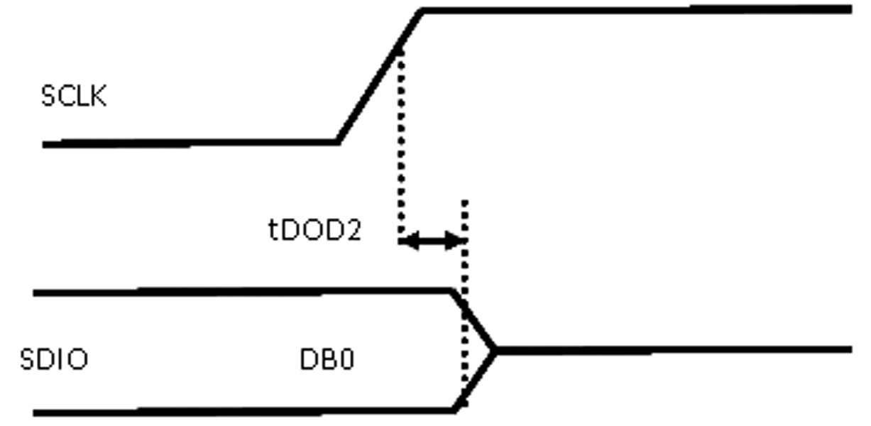 Figure 3. SDO Disable Time After 16th Rise Edge of SCLK
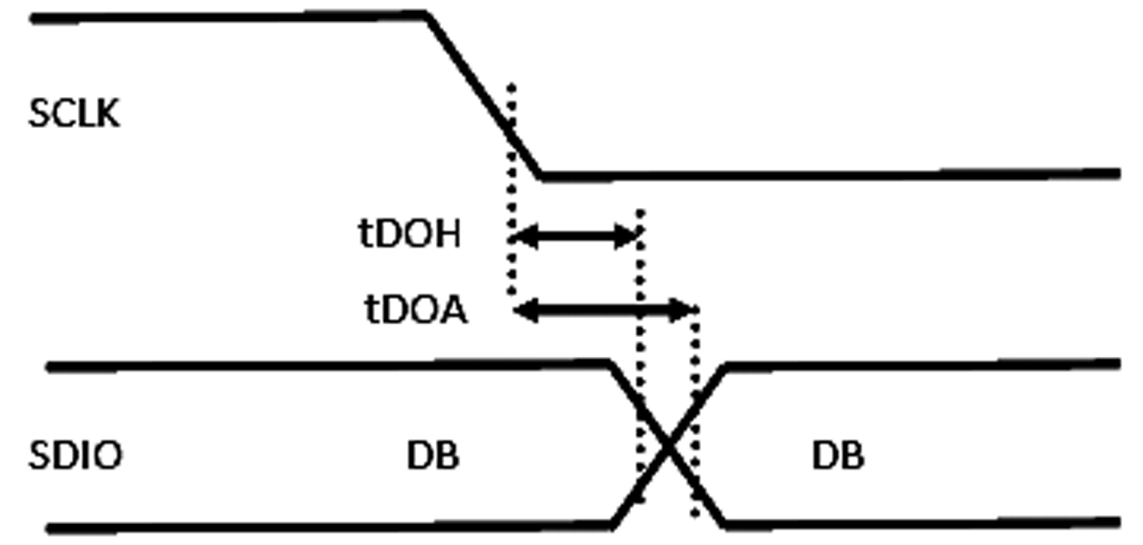 Figure 4. SDO Access Time (tDOA) and SDO Hold Time (tDOH) After the Fall Edge of SCLK
 Figure 5. SDO Enable Time from the Fall Edge of 8th SCLK
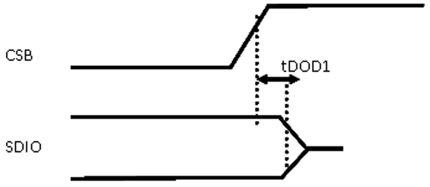 Figure 6. SDO Disable Time after Rise Edge of CSB
 Figure 7. SDO Rise and Fall Times
7.8 Typical Characteristics
VDD = +3.3 V, VCM = 1.15 V, and TA = 25°C unless otherwise noted Figure 8. Gain = 167 V/V vs. Temperature
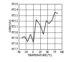 Figure 10. Gain = 669 V/V vs. Temperature
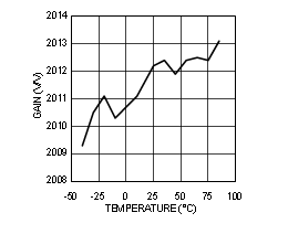 Figure 12. Gain = 2004 V/V vs. Temperature
 Figure 14. Output Offset vs. Temperature
 Figure 16. Input Bias Current vs. Temperature
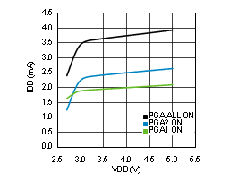 Figure 18. Supply Current vs. Supply Voltage
 Figure 20. Output Offset vs. Supply Voltage
 Figure 9. Gain = 335 V/V vs. Temperature
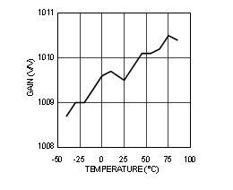 Figure 11. Gain = 1002 V/V vs. Temperature
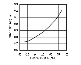 Figure 13. Phase Delay vs. Temperature
 Figure 15. Common-Mode Voltage vs. Temperature
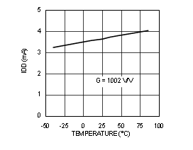 Figure 17. Supply Current vs. Temperature
 Figure 19. Power-Down Supply Current vs. Supply Voltage